Semiconductor device

A semiconductor and wiring technology, applied in the direction of semiconductor devices, semiconductor/solid-state device parts, electric solid-state devices, etc., can solve the problems of solder bump connection strength weakening, connection part cracks, etc., to achieve miniaturization and thinning, production High efficiency and improved electromigration properties

Active Publication Date: 2010-09-15
GK BRIDGE 1
View PDF4 Cites 4 Cited by
  • Summary
  • Abstract
  • Description
  • Claims
  • Application Information

AI Technical Summary

Problems solved by technology

[0006] Flip-chip connection can achieve faster signal transmission between semiconductor elements and wiring boards than wire bonding connections, but as the number of pads o...

Method used


Image

  • Semiconductor device
  • Semiconductor device
  • Semiconductor device

Examples


Embodiment 1

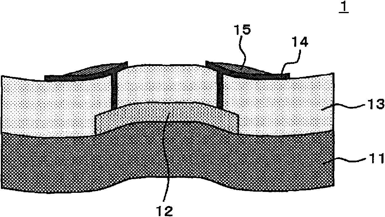
[0076] A semiconductor device according to Embodiment 1 of the present invention will be described with reference to the drawings. figure 1 It is a cross-sectional view schematically showing the structure of the semiconductor device according to Embodiment 1 of the present invention.

[0077] The semiconductor device 1 of the first embodiment is a package in which a semiconductor element 12 is embedded in a wiring substrate (support substrate 11 , buried insulating layer 13 , and fan-out wiring (Fan out wiring) 14 ). The semiconductor device 1 has a wiring thickness reinforcing portion 15 in a predetermined region above the outer peripheral portion of the semiconductor element 12 for preventing cracks in the embedded insulating layer 13 on the outer peripheral portion of the semiconductor element 12 .

[0078] The semiconductor element 12 is a semiconductor chip (for example, a silicon semiconductor element, etc.), and a plurality of pads (not shown) are provided on one surfac...

Embodiment 2

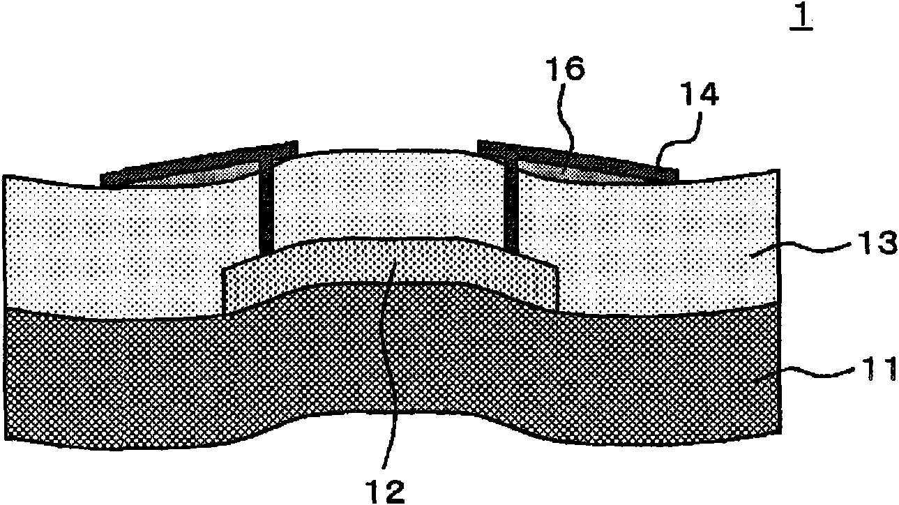
[0090] A semiconductor device according to Embodiment 2 of the present invention will be described with reference to the drawings. figure 2 It is a cross-sectional view schematically showing the structure of a semiconductor device according to Embodiment 2 of the present invention.

[0091] In the semiconductor device of Embodiment 2, instead of the wiring thickness reinforcing portion ( figure 1 The insulating layer thickness reinforcing portion 16 in 15) is used to prevent cracks in the embedded insulating layer 13 on the outer peripheral portion of the semiconductor element 12 . The insulating layer thickness reinforced portion 16 is arranged between the embedded insulating layer 13 and the fan-out wiring 14 . Other structures are the same as in Embodiment 1.

[0092] The insulating layer thickness reinforced portion 16 is provided vertically above the outer peripheral portion of the semiconductor element 12 and may be formed of an insulating material that forms an insul...

Embodiment 3

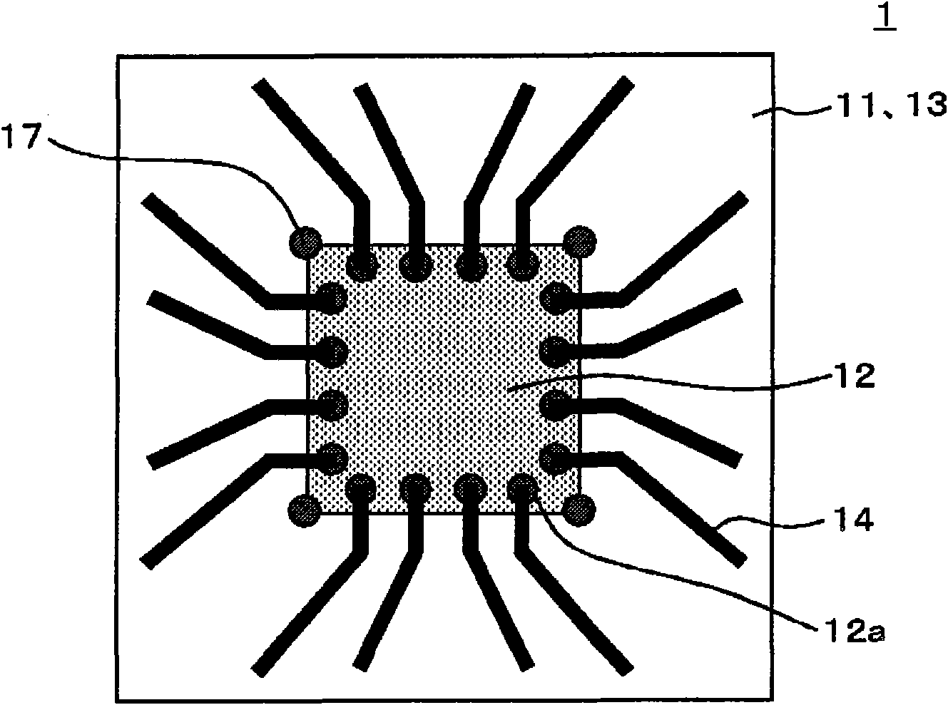
[0096] A semiconductor device according to Embodiment 3 of the present invention will be described with reference to the drawings. image 3 It is a cross-sectional view schematically showing the structure of a semiconductor device according to Embodiment 3 of the present invention.

[0097] The semiconductor device of Example 3 is a package in which a semiconductor element 12 is embedded in a wiring substrate (support substrate 11 , embedded insulating layer 13 , fan-out wiring 14 ). In order to prevent cracks in the buried insulating layer 13 on the outer peripheral portion of the semiconductor element 12, the semiconductor device 1 has a reinforcing via wiring 17 connected to at least one end (corner) of the semiconductor element 12 and not connected to the fan-out Wiring 14 is connected.

[0098] The semiconductor element 12 is a semiconductor chip (for example, a silicon semiconductor element, etc.), and a plurality of pads (not shown) are provided on one surface. The se...


PUM

PropertyMeasurementUnit
Thicknessaaaaaaaaaa
Thermal expansion coefficientaaaaaaaaaa

Abstract

Provided is a higher density, thinner and lower cost semiconductor device by eliminating reliability failure due to concentration of internal stress in a final semiconductor device. The semiconductor device is provided with a semiconductor element; a supporting substrate, which is arranged on a surface opposite to a surface whereupon a pad of the semiconductor element is arranged, and has an area larger than that of the semiconductor element; an embedding insulating layer for embedding the semiconductor element on the supporting substrate; a fan-out wiring lead out from the pad to a region on the outer circumference side of the semiconductor element on the embedding insulating layer; and a wiring thickness reinforcing section, which is arranged in a prescribed region above the outer circumference section of the semiconductor element for reinforcing mechanical strength of the embedding insulating layer and the fan-out wiring.

Description

technical field [0001] Description of the relevant application [0002] The present invention is based on and claims priority to the prior Japanese Patent Application No. 2007-273929 (filed on October 22, 2007), and the entire content of the prior application is described in this specification by reference. [0003] The present invention relates to a semiconductor device incorporating a semiconductor element. Background technique [0004] With the continuous miniaturization of electronic equipment, the miniaturization and integration of semiconductor elements themselves, as well as the high-density mounting technology in semiconductor packages, are progressing day by day. Conventionally, in the packaging of semiconductor elements, there are wire bonding connections using gold wires or the like and flip chip connections using solder balls or the like as methods of connecting the wiring board of the package and the semiconductor elements. [0005] Although the wire bonding c...

Claims


Application Information

Patent Timeline
IPC IPC(8): H01L23/12
CPCH01L2924/01046H01L2924/01082H01L2924/01041H01L23/49822H01L2924/01004H01L2924/3511H01L24/20H01L2924/01038H01L2924/01019H01L23/49827H01L2924/15311H01L24/19H01L2924/01029H01L2924/19041H01L2924/01013H01L23/49838H01L2924/01056H01L2224/20H01L2924/01047H01L2924/01079H01L2924/0104H01L2224/04105H01L2924/01005H01L2924/01033H01L2924/01006H01L2924/0102H01L2924/01074H01L2924/01078H01L2924/01042H01L2924/01057H01L2924/01073H01L23/5389H01L2924/1461H01L2924/00H01L23/5226H01L23/528
Inventor 山道新太郎森健太郎村井秀哉
Owner GK BRIDGE 1
Why Eureka
Try Eureka