Detection device and method for high-power semiconductor laser

A technology of semiconductors and lasers, which is applied in the field of testing devices for high-power semiconductor laser modules. It can solve the problems of solid-state laser beam quality degradation, drift, and uneven heat distribution of the pump laser medium, and achieves convenient operation, low cost, and accurate measurement. Effect

Inactive Publication Date: 2012-02-15
SHANGHAI INST OF OPTICS & FINE MECHANICS CHINESE ACAD OF SCI
View PDF0 Cites 0 Cited by
  • Summary
  • Abstract
  • Description
  • Claims
  • Application Information

AI Technical Summary

Problems solved by technology

In many application fields, it is necessary to side pump the laser medium (rod), so there is a high-power semiconductor laser module with a semi-circular or circular packaging structure. At present, it is only possible to test each high-power semiconductor laser module before packaging. The performance of the semiconductor laser is used to infer the performance of the package after forming. The power performance after the package will not be greatly affected, but its wavelength will drift

Method used


Image

  • Detection device and method for high-power semiconductor laser
  • Detection device and method for high-power semiconductor laser
  • Detection device and method for high-power semiconductor laser

Examples


Embodiment Construction

[0025] The present invention will be further described below with reference to the embodiments and accompanying drawings.

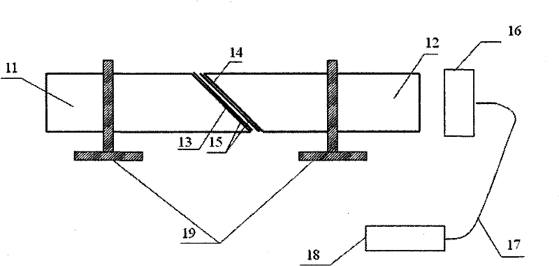
[0026] see first figure 1 , figure 1 It is a structural schematic diagram of Embodiment 1 of the present invention; the test device of the high-power semiconductor laser module of this embodiment includes a test rod, a test rod fixing fixture 19, a focusing lens 16, a light guide fiber 17 and a detector 18, and the test rod It is composed of two crystals or glass rods with the same structure that have 45° oblique sections 13 and 14 at one end and are coated with a high reflection film 15 to the laser diode wavelength, and the other end section is a perfect circular surface, and the oblique sections 13 and 14 Relatively coaxially glued together, the test rod is placed on the test rod fixing fixture 19, the focusing lens 16 is arranged outside one end of the test rod, and one end of the light guide fiber 17 is located on the The focal point of the focusin...


PUM


Abstract

The invention discloses detection device and method for a high-power semiconductor laser. The device comprises a test bar, a test bar fixing clamp, a condenser lens, a light guide optical fiber and a detector; the test bar is formed by gluing oblique sections of two transparent material bars with the same structure in an opposite and coaxial way, wherein one end of each transparent material bar has a 45 degree oblique section and is plated with a high reflective film specific to the wavelength of a laser diode, and the other end of each transparent material bar has a regular round section; the test bar is arranged on the test bar fixing clamp; the condenser lens is arranged outside one end or two ends of the test bar; and one end of the light guide optical fiber is positioned at the focusof the condenser lens and the other end is connected with the input end of the detector. The invention is applicable to the measurement of high-power semiconductor laser modules of semi-circle shapedor circle shaped packaging structures and has the advantages of simple structure and convenient test operation.

Description

technical field [0001] The invention relates to a high-power semiconductor laser module, in particular to a testing device and method for a high-power semiconductor laser module. Background technique [0002] High-power semiconductor lasers have the advantages of small size, high efficiency, low threshold, and long working life. They are used as solid-state laser pump light sources or direct light sources and have entered the development system. High-power semiconductor laser arrays with kilowatts have also directly entered the industry. application. In many application fields, it is necessary to side pump the laser medium (rod), so there is a high-power semiconductor laser module with a semi-circular or circular packaging structure. At present, it is only possible to test each high-power semiconductor laser module before packaging. The performance of the semiconductor laser is used to infer the performance of the package after forming. The power performance after the packa...

Claims


Application Information

Patent Timeline
IPC IPC(8): G01J9/00G01J1/00
Inventor 辛国锋瞿荣辉蔡海文方祖捷陈高庭沈力皮浩洋
Owner SHANGHAI INST OF OPTICS & FINE MECHANICS CHINESE ACAD OF SCI
Why Eureka
Try Eureka