Substrate heat processing apparatus

A technology for heat treatment devices and substrates, applied in optics, instruments, and optomechanical equipment, can solve the problems of time-consuming cooling tubes, limited bending of cooling tubes, and inability to reduce the thickness of cooling plates, so as to increase the number of storage, improve rigidity, The effect of increasing hardness

Active Publication Date: 2012-07-04
TOKYO ELECTRON LTD
View PDF2 Cites 0 Cited by
  • Summary
  • Abstract
  • Description
  • Claims
  • Application Information

AI Technical Summary

Problems solved by technology

[0010] In addition, in the structure described in Patent Document 2, since the cooling pipe needs to have a certain wall thickness, the thickness of the cooling plate cannot be reduced.
In addition, the degree of bending of the cooling pipe is limited, so there is a problem that it takes time and labor to install the cooling pipe

Method used


Image

  • Substrate heat processing apparatus
  • Substrate heat processing apparatus
  • Substrate heat processing apparatus

Examples


Embodiment Construction

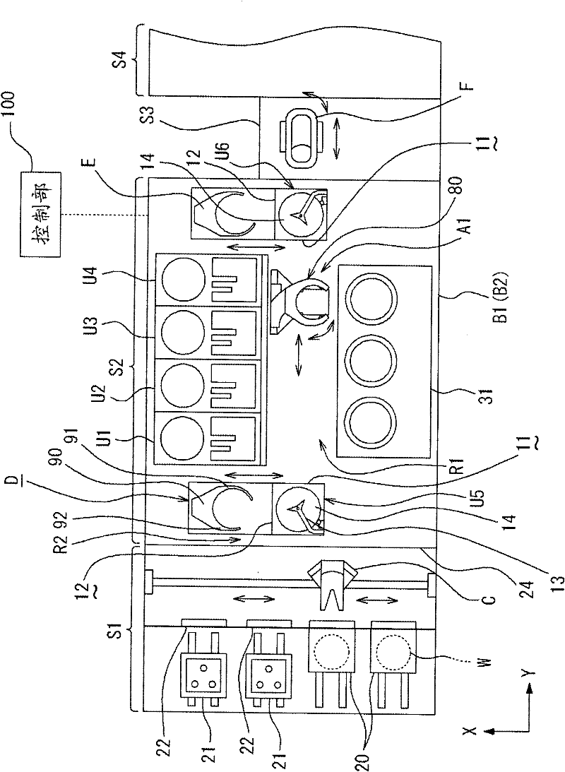
[0047] Hereinafter, embodiments of the present invention will be described in detail with reference to the drawings. Here, a case where the substrate heat treatment apparatus of the present invention is applied to a resist coating / development processing apparatus for semiconductor wafers will be described.

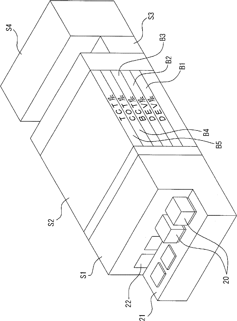
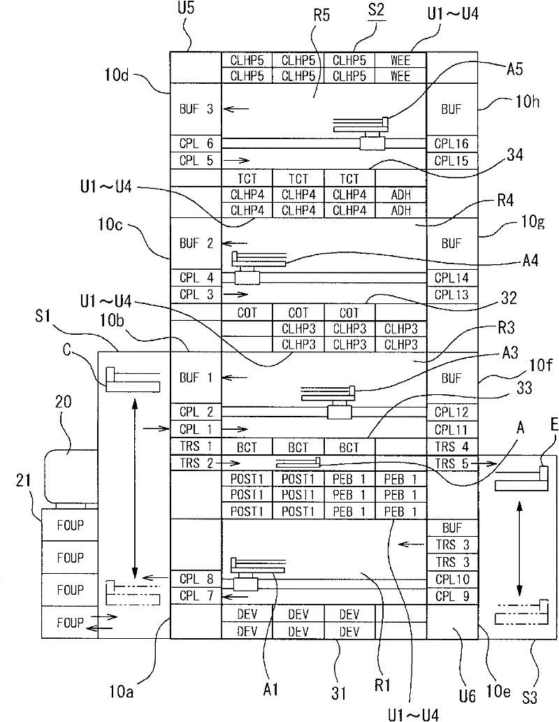
[0048] The above-mentioned resist coating and developing treatment apparatus such as Figure 1 to Figure 8 As shown, it includes: carrier block S1, which is used for loading and unloading carrier 20, which is sealed and accommodated, for example, 13 semiconductor wafers W (hereinafter referred to as wafer W) as substrates; processing block S2, which is arranged vertically A plurality of, for example, five unit blocks B1 to B5; an interface block S3; and an exposure device S4 as a second processing block.

[0049] The above-mentioned carrier block S1 is provided with a mounting table 21 capable of mounting a plurality of (for example, 4) carriers 20, an opening and closing...


PUM


Abstract

The present invention provides a substrate heat processing apparatus, which can reduce the configuration space of a heat processing plate as possible thereby realizing the miniaturization of device, increasing the number of accommodated substrates and increasing the freedom and productivity of the heat medium flow. The substrate heat processing apparatus is provided with a heat processing plate such as a cooling plate (14), which is used for carrying a semiconductor wafer (W) and performing heat processing to the wafer to a preset temperature, wherein, the cooling plate (14) is provided with a cooling plate body (64). The cooling plate body (64) is obtained through laminating a plurality of thin plates (1) composed of heat-conductive material through a mode such as diffusion joint mode, and is provided with a supplying flow path (61a) and discharging flow path (62a) of the heat medium, a refrigerant flow path (63) and adsorption holes (64f), which are provided through laminating the thin plates (1).

Description

technical field [0001] The present invention relates to a substrate heat treatment device such as a semiconductor wafer, a flat panel display substrate (FPD substrate, flat panel display) and the like. Background technique [0002] Generally, in the photolithography technique, a series of processes described below are performed. That is, a photoresist is applied on a substrate, a resist film thus formed is exposed according to a predetermined circuit pattern, and the exposed pattern is developed to form a desired circuit pattern on the resist film. . [0003] This processing method generally includes a resist coating processing unit, a heating processing unit, a cooling processing unit, and a development processing unit in a state of laminating multiple layers independently; the above resist coating processing unit applies the resist liquid to The heat treatment unit heats the substrate on which the resist coating process and the exposure treatment have been performed; the...

Claims


Application Information

Patent Timeline
Patent Type & Authority Patents(China)
IPC IPC(8): H01L21/00
CPCG03F7/168G03F7/40G03F7/70716H01L21/324H01L21/67098
Inventor 水永耕市
Owner TOKYO ELECTRON LTD
Why Eureka
Try Eureka