High-power fundamental transverse mode flat plate coupling optical waveguide semiconductor laser structure

A fundamental transverse mode, high-power technology, applied in the direction of semiconductor lasers, lasers, laser components, etc., can solve the problems of unfavorable industrialization, high cost, and difficult production

Inactive Publication Date: 2010-09-22
INST OF SEMICONDUCTORS - CHINESE ACAD OF SCI
View PDF0 Cites 7 Cited by
  • Summary
  • Abstract
  • Description
  • Claims
  • Application Information

AI Technical Summary

Problems solved by technology

However, compared with edge-emitting semiconductor lasers, the material preparation and device fabrication of vertical-cavity surface-emitting semiconductor lasers are difficult and costly, which is not conducive to industrialization

Method used


Image

  • High-power fundamental transverse mode flat plate coupling optical waveguide semiconductor laser structure
  • High-power fundamental transverse mode flat plate coupling optical waveguide semiconductor laser structure
  • High-power fundamental transverse mode flat plate coupling optical waveguide semiconductor laser structure

Examples


Embodiment Construction

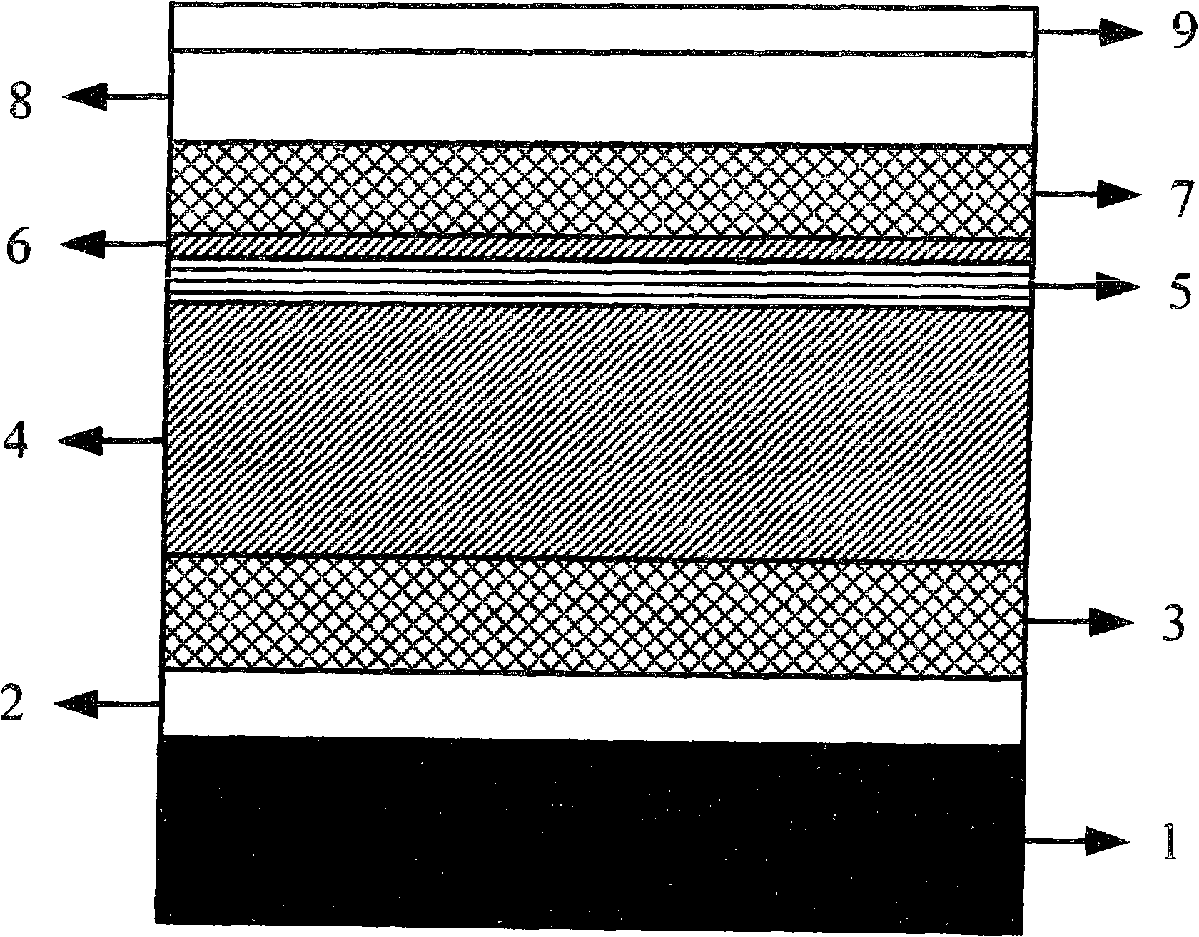
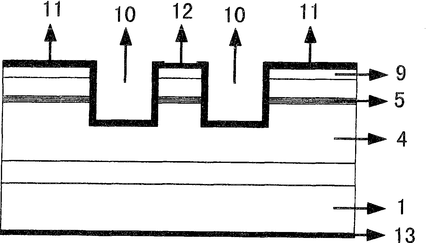
[0031] Combine below figure 1 and figure 2 The details of the structure of a high-power fundamental transverse mode slab-coupled optical waveguide semiconductor laser according to a specific embodiment of the present invention will be described in detail.

[0032] Step 1: Follow the figure 1 The structure shown undergoes epitaxial growth of the material.

[0033] see figure 1 As shown, the structure of a high-power fundamental transverse mode slab-coupled optical waveguide semiconductor laser in this embodiment includes:

[0034] -Substrate 1, the substrate 1 is used to carry out the epitaxial growth of each layer of laser material on it, the substrate 1 is N-type gallium arsenic on the (100) plane, which is beneficial to the injection of electrons and reduces the series connection of substrate materials resistance;

[0035] - buffer layer 2, which is made on the substrate 1 and is an N-type gallium arsenide material, its purpose is to form a high-quality epitaxial surfa...


PUM


Abstract

The invention discloses a high-power fundamental transverse mode flat plate coupling optical waveguide semiconductor laser structure which comprises a substrate, a buffer layer, an N-type lower limiting layer, a lower waveguide layer, an active area, an interface layer, a P-type upper limiting layer, an intermediate layer, an electrode contract layer, a double channel, a passivating film layer, a P side electrode and an N side electrode. The substrate is used for the growth of all epitaxial layer materials of the laser on the substrate; the buffer layer is made on the substrate; the N-type lower limiting layer is made on the buffer layer; the lower waveguide layer is made on the N-type lower limiting layer; the active area is made on the lower waveguide layer; the interface layer is made on the active area; the P-type upper limiting layer is made on the interface area; the intermediate layer is made on the P-type limiting layer; the electrode contact layer is made on the intermediate layer; the double channel is etched on the electrode contact layer, the etching depth is kept within the lower waveguide layer, and a ridge-type table top is formed in the middle of the double channel; the passivating film layer is made on the upper surface of the electrode contact layer and the bottom and the two sides of the double channel and the passivating film layer on the ridge-type table top is disconnected; the P side electrode is made on the ridge-type table top and is in contact with the electrode contact layer; and the N side electrode is made under the substrate.

Description

technical field [0001] The invention relates to a high-power fundamental transverse mode semiconductor quantum well laser structure, in particular to a high-power fundamental transverse mode flat-plate coupled optical waveguide semiconductor laser structure. Background technique [0002] With the development of optoelectronic industry, the application of semiconductor laser is more and more extensive. In particular, high-power fundamental transverse mode semiconductor lasers are widely used in optical fiber communication systems, laser medical and health care equipment, and single-mode fiber lasers. Especially for the 980nm semiconductor laser pump source used in the erbium-doped fiber amplifier, it is required to be coupled with a single-mode fiber, and its good beam quality and circular spot are more important for improving the fiber coupling efficiency. It is the hardware basis and key device to realize the function of Erbium-doped fiber amplifier (EDFA) in the optical f...

Claims


Application Information

Patent Timeline
Patent Type & Authority Applications(China)
IPC IPC(8): H01S5/00H01S5/065H01S5/068H01S5/10
Inventor 熊聪王俊崇锋刘素平马骁宇
Owner INST OF SEMICONDUCTORS - CHINESE ACAD OF SCI
Why Eureka
Try Eureka