Probe and manufacturing method thereof

A manufacturing method and probe technology, which are applied in measuring devices, instruments, measuring electricity and other directions, can solve the problems of cracking, the durability of the probe cannot be improved, and detection errors, so as to reduce the manufacturing cost, solve the test accuracy, and prolong the use. effect of life

Inactive Publication Date: 2012-10-03
HUAYING OPTOELECTRONICS
View PDF0 Cites 0 Cited by
  • Summary
  • Abstract
  • Description
  • Claims
  • Application Information

AI Technical Summary

Problems solved by technology

In other words, the conventional probe block 100 uses a small margin (Margin) during detection, and when the offset exceeds this margin, the bumps 120 on the probe block 100 will contact other test pads 210 , causing detection errors
[0009] In addition, because the bumps produced by the conventional technology cannot be formed on the leads accurately, there is a gap between the bumps and the leads, and when the bumps are in contact with the test pads, the bumps may not be aligned correctly. Lateral force caused by aligning the test pad may cause the bump to crack from the gap, making the probe unusable
Therefore, the durability of conventional probes cannot be improved, and what's more, it may also cause false detection results

Method used


Image

  • Probe and manufacturing method thereof
  • Probe and manufacturing method thereof
  • Probe and manufacturing method thereof

Examples


Embodiment Construction

[0041] A preferred embodiment of the present invention will be described in detail with the accompanying drawings and the following description. In different drawings, the same reference numerals represent the same or similar components. The probes of the present invention are not limited to the testing of liquid crystal display panels, and other probe cards such as integrated circuit testing, or probe structures that need to be manufactured with tiny dimensions can be implemented. The embodiments described below are for illustration only, and therefore the scope of the present invention is not limited thereto.

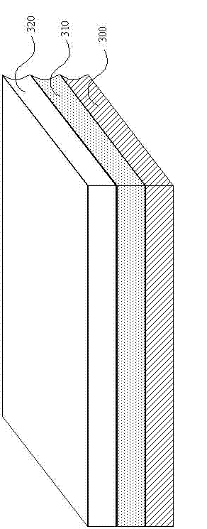
[0042] Figure 3 to Figure 8 It is a three-dimensional side view of the probe manufacturing steps according to a preferred embodiment of the present invention. Figure 3 to Figure 8 A method of manufacturing a probe according to a preferred embodiment of the present invention is described, which shows a process of manufacturing the probe according to a preferred embo...


PUM


Abstract

The invention discloses a probe and a manufacturing method thereof. The probe comprises a leading wire and a lug, wherein the leading wire is formed on a substrate, and the lug is formed on the leading wire. In addition, the invention also discloses a probe block which comprises a plurality of probes arranged on the substrate, thus the probe block comprises a plurality of leading wires and a plurality of lugs. Each lug is arranged right above one end of each leading wire. The lug and the leading wire of the probe according to the invention are formed integrally. The manufacturing method of the probe is characterized in that the leading wire of the probe and the lug formed on the leading wire are manufactured by one gray scale photo mask processing on the substrate. The invention solves the problem that the common two photo mask processing can possibly result in crack of the lug, thereby prolonging the service life of the probe and solving the problem of testing accuracy.

Description

technical field [0001] The present invention relates to a probe and a manufacturing method thereof, in particular to a probe for testing a liquid crystal display panel and a manufacturing method thereof. Background technique [0002] A probe is a device used to measure the electrical characteristics of tiny electronic components (for example, semiconductor components or thin-film transistor arrays in liquid crystal display panels). As is well known in the art, a thin film transistor array (Thin Film Transistor Array, TFT Array) has a plurality of gate lines and signal lines connected to a plurality of test pads (Test Pad) for exchanging with an external electronic system Signal. The thin film transistor array processes the electrical signals input through the test pads, and transmits the processed results to an external system through the test pads to detect the quality or defects of the electrical characteristics of the display panel. [0003] During this period, a plura...

Claims


Application Information

Patent Timeline
Patent Type & Authority Patents(China)
IPC IPC(8): G01R1/073
Inventor 邱俊郎洪仁财黄铭岗林志坤
Owner HUAYING OPTOELECTRONICS
Why Eureka
Try Eureka