Inorganic light-emitting diode display device
A technology of light-emitting diodes and optical devices, which is applied to electrical components, electrical solid-state devices, circuits, etc., can solve problems such as difficulty in realizing projection display efficiency, and achieve the effect of increasing the effective display area and reducing heat generation.
- Summary
- Abstract
- Description
- Claims
- Application Information
AI Technical Summary
Problems solved by technology
Method used
Image
Examples
Embodiment 1
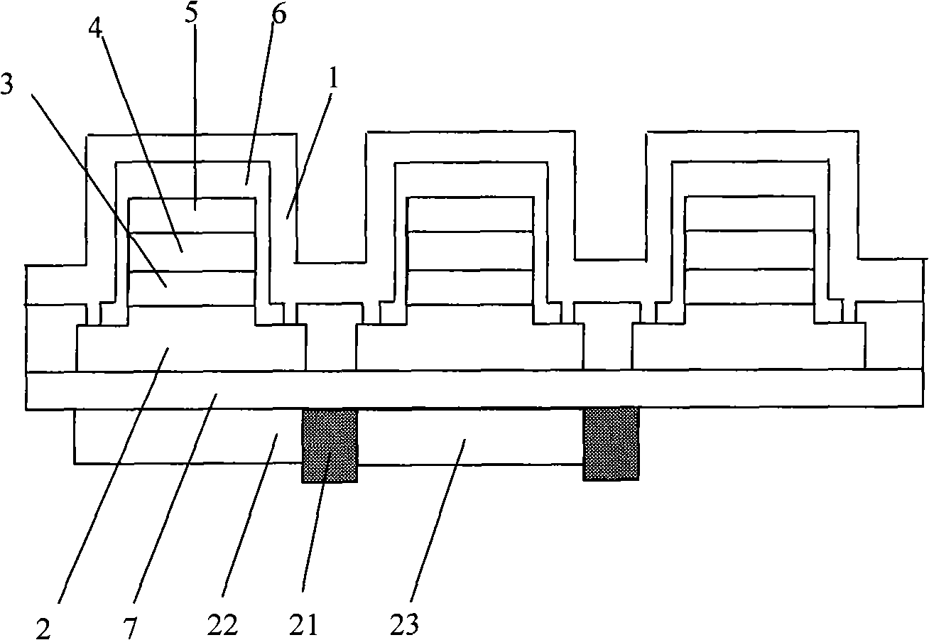
[0037] figure 1 A structural schematic diagram of a passive matrix driven inorganic light emitting diode matrix display device is shown. Such as figure 1 As shown, the inorganic light-emitting diode matrix display device includes: electronic conductive electrodes and lead wires 1, electronic conductive layer 2 of inorganic light-emitting diodes, light-emitting layer 3 of inorganic light-emitting diodes, hole-type conductive layers 4 of inorganic light-emitting diodes, inorganic light-emitting diodes Hole-type electrodes and leads 5 of the light-emitting diode, insulating layer 6 , substrate 7 , black matrix 21 , red photo-conversion luminescent film 22 , and green photo-conversion luminescent film 23 .
[0038] Among them, the electronic conductive electrode and the lead wire 1 are made of metal materials titanium (Ti) and aluminum (Al), each semiconductor layer of the inorganic light emitting diode (including the electronic conductive layer 2 of the inorganic light emitting ...
Embodiment 2
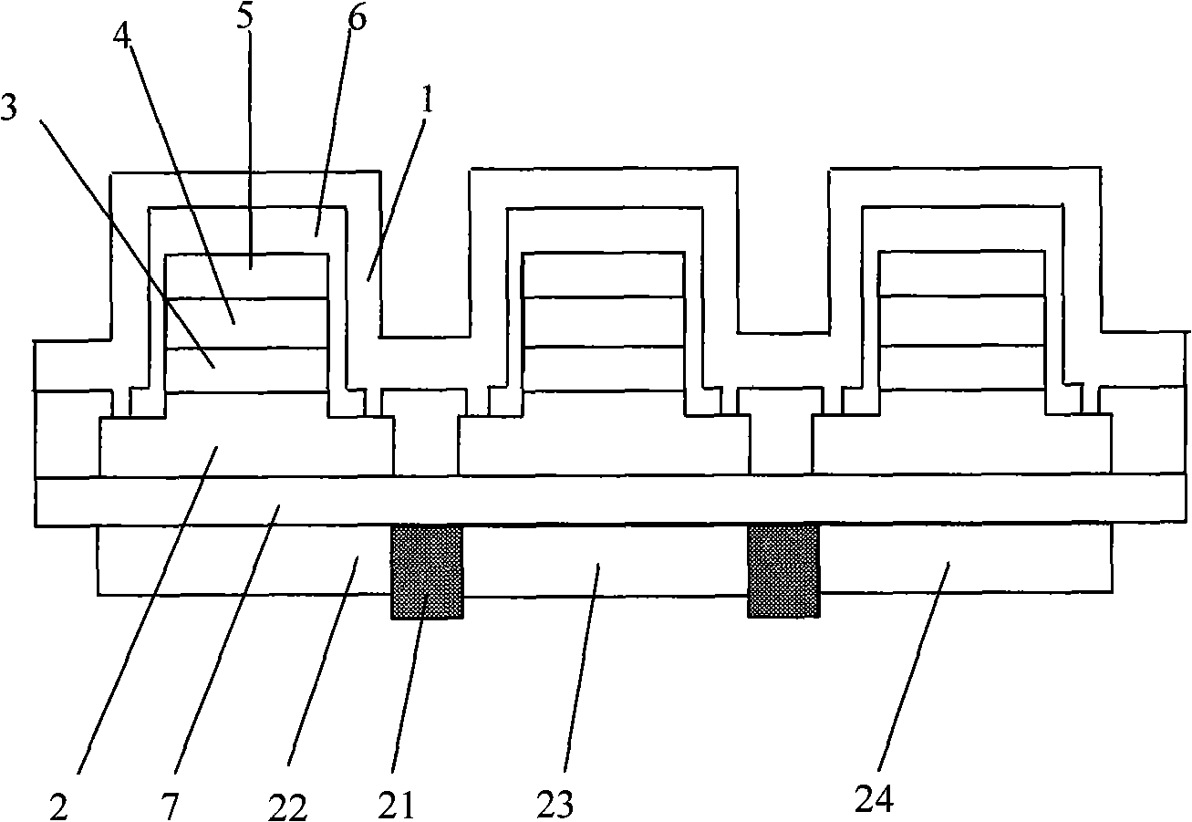
[0053] figure 2 A structural schematic diagram of another inorganic light-emitting diode matrix display device driven by a passive matrix is shown. figure 2 The display device shown with the figure 1 The display device shown is substantially the same except that a blue absorbing optical film 24 is also included. The blue absorptive optical film 24 is made of materials such as phthalo-bronze and its derivatives dispersed in photosensitive resin (such as acrylic). In addition to the steps in Example 1, its specific manufacturing steps also include a step of making a blue absorptive optical film, that is, to make a blue absorptive optical film 24 by coating (acrylic-based acrylic phthalo-bronze dispersed in In the photosensitive resin), the pattern corresponding to the blue sub-pixel is formed by exposure and etching.
[0054] In the case of electronic electrodes and lead wires in one direction driven by this passive matrix, signals are applied to hole-type electrodes and ...
Embodiment 3
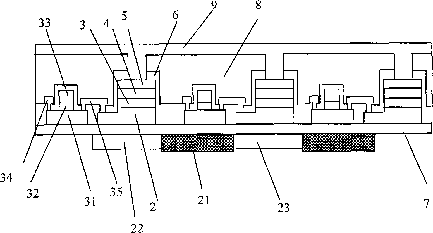
[0056] The inorganic light emitting diode matrix display device in the third embodiment is basically the same as the inorganic light emitting diode matrix display device in the second embodiment. The permanent optical film 24 is replaced by a blue photoconversion luminescent film 24. The blue photosensitive conversion luminescent film 24 is made of gallium nitride (ie (Al)Ga(In)N) semiconductor material doped with aluminum and indium, and its specific manufacturing process is: the method of metal-organic chemical vapor deposition to produce green light The electroconverting luminescent film 24 is formed by a stripping method corresponding to the photoluminescence required by the blue sub-pixel.
[0057] In the passive matrix-driven display matrix, when the electron-type electrodes and leads in one direction of the display matrix are gated, the hole-type electrodes and leads in the other direction are applied with signals, and the inorganic light-emitting diodes that cross the ...
PUM
 Abstract
Description
Claims
Application Information


