Low-voltage resistive random access memory and preparation method thereof

A resistive variable memory and resistive variable technology, applied in the direction of electrical components, etc., can solve the problems of increasing process steps, high turn-on voltage and turn-off voltage, difficulties, etc., to achieve large application prospects, turn-off current optimization, low resistance variable voltage and resistance The effect of variable current

Active Publication Date: 2010-10-06
SEMICONDUCTOR MANUFACTURING INTERNATIONAL (BEIJING) CORP +1
View PDF3 Cites 10 Cited by
  • Summary
  • Abstract
  • Description
  • Claims
  • Application Information

AI Technical Summary

Problems solved by technology

Such substances are generally compatible with the CMOS process and can exhibit good resistive switching characteristics. However, compared with conventional processes, some process steps are often required
SiO 2 As a material that is fully compatible with the traditional CMOS process, it also shows good resistance switching characteristics under certain conditions, but it needs high temperature treatment, which brings difficulties to its practical application.
The applicant found through research: by going to SiO 2 Introducing Si into the silicon, so as to achieve the purpose of introducing defects and controlling defects, and successfully realized the resistive variable memory under low temperature process. The prepared resistive variable memory based on SiO has good resistive characteristics, but its turn-on voltage and turn-off voltage are both low. High, there is still a certain gap with the actual application

Method used


Image

  • Low-voltage resistive random access memory and preparation method thereof
  • Low-voltage resistive random access memory and preparation method thereof
  • Low-voltage resistive random access memory and preparation method thereof

Examples


Embodiment 1

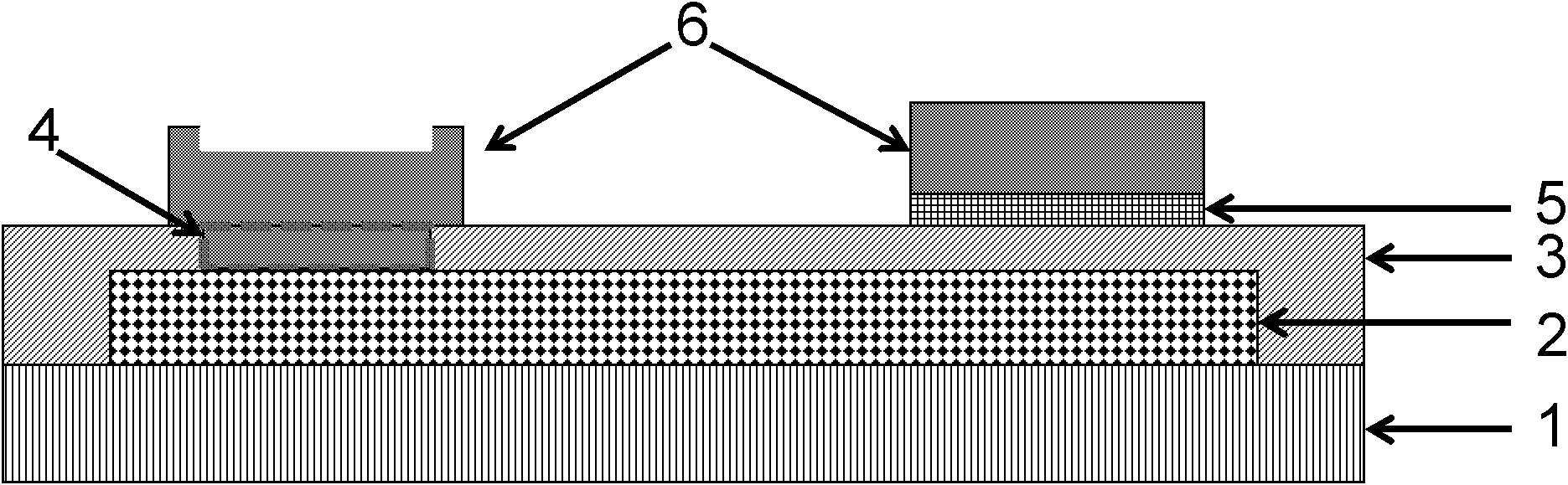
[0028] The schematic diagram of the cross-sectional structure of the resistive memory made in this embodiment is as follows: figure 1 As shown, the preparation process of the resistive variable memory of this example is described below in combination with the schematic cross-sectional structure.

[0029] 1) First, a layer of W metal is prepared on the silicon substrate 1 by physical vapor deposition (PVD) method or other film-forming methods in the IC process, and the bottom electrode is patterned using standard photolithography techniques to form the bottom electrode 2 .

[0030] 2) Adjust N in PECVD 2 O and SiH 4 The ratio of gas flow to SiH 4 :N 2 O=50:100, the resistive material layer SiO was prepared 0.4 N 0.4 . The PECVD process parameters are as follows: power=60W, air pressure=550mtorr, temperature=300°C.

[0031] 3) Define the bottom electrode lead-out hole by photolithography and etching;

[0032] 4) Same as the bottom electrode, the top electrode and its pr...

Embodiment 2

[0041] 1) First, a layer of W metal is prepared on the silicon substrate 1 by physical vapor deposition (PVD) method or other film-forming methods in the IC process, and the bottom electrode is patterned using standard photolithography techniques to form the bottom electrode 2 .

[0042] 2) Adjust N in PECVD 2 O and SiH 4 The ratio of gas flow to SiH 4 :N 2 O=30:150, the resistive material layer SiO was prepared 0.7 N 0.5 . The PECVD process parameters are as follows: power=60W, air pressure=550mtorr, temperature=300°C.

[0043] 3) Define the bottom electrode lead-out hole by photolithography and etching

[0044] 4) The top electrode and its protective electrode are prepared by PVD method or other film-forming methods in the IC process, and the protective electrode is platinum, titanium or gold.

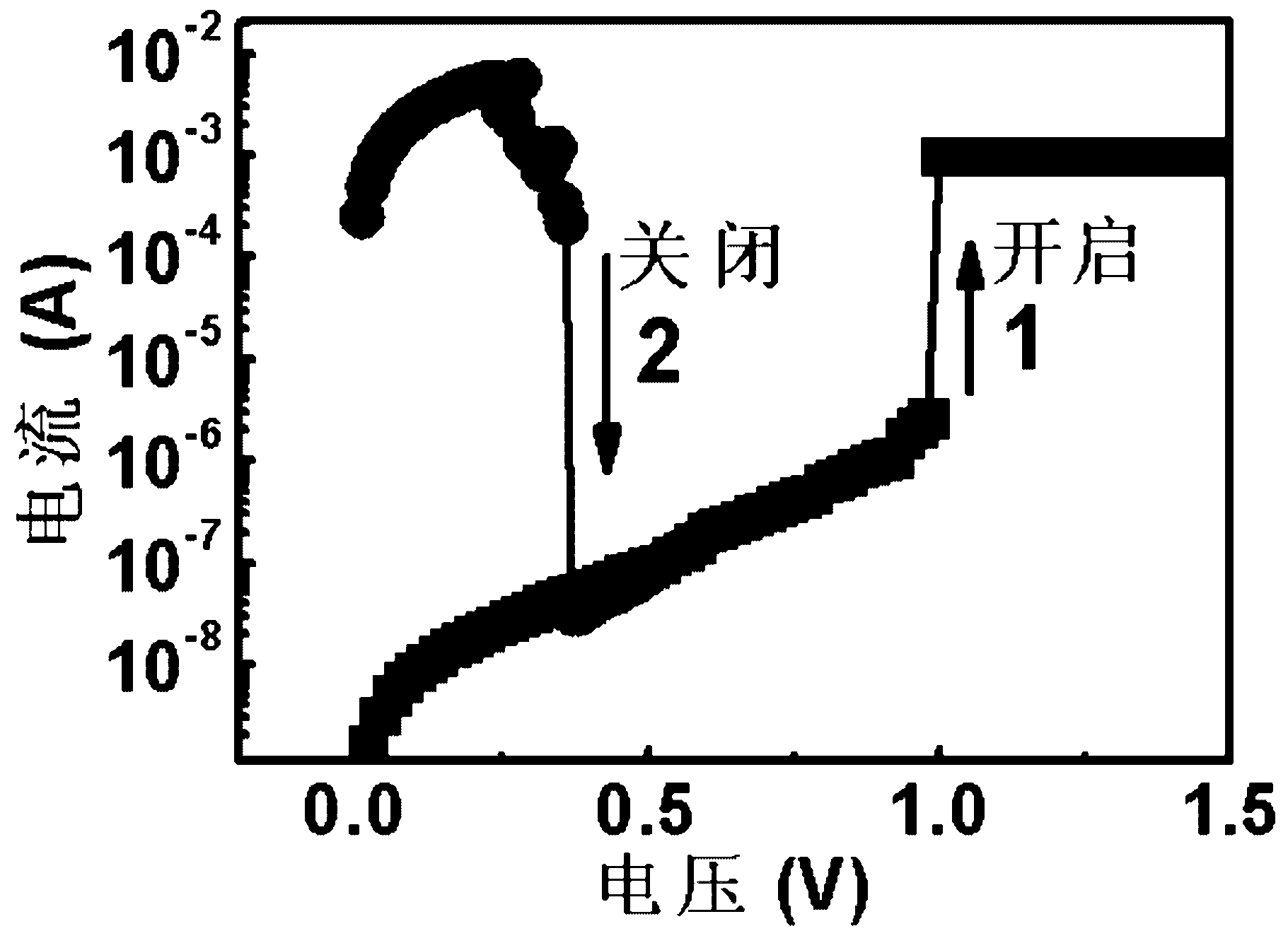
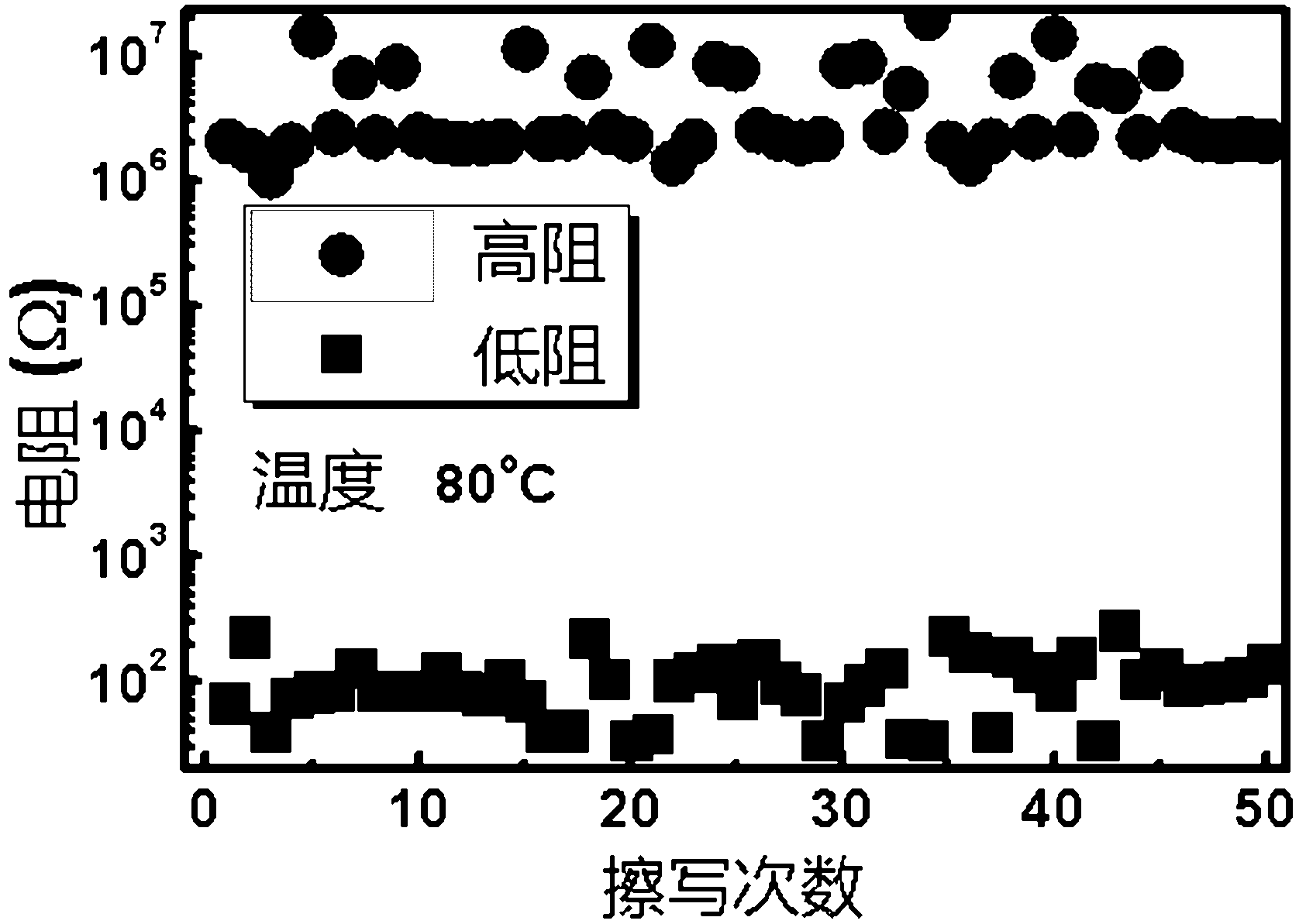
[0045] The resistive memory (W / SiO 0.7 N 0.5 / Cu) is similar to the resistive memory made in Example 1 in its resistive characteristics, erasable characteristics and retent...

Embodiment 3

[0047] 1) First, a layer of Pt metal is prepared on the silicon substrate 1 by PVD method or other film-forming methods in the IC process, and the bottom electrode is patterned using standard photolithography techniques to form the bottom electrode 2 .

[0048] 2) Adjust N in PECVD 2 O and SiH 4 The proportion of SiH 4 :N 2 O=14:150, the resistive material layer SiON was prepared 0.6 . The PECVD process parameters are as follows: power=60W, air pressure=550mtorr, temperature=300°C.

[0049] 3) Define the bottom electrode lead-out hole by photolithography and etching;

[0050] 4) The top electrode and its protective electrode are prepared by PVD method or other film-forming methods in the IC process, and the protective electrode is platinum, titanium or gold.

[0051] The resistive memory (Pt / SiON) prepared in this embodiment 0.6 / Cu) is similar to the resistive memory made in Example 1 in its resistive characteristics, erasable characteristics and retention characterist...


PUM


Abstract

The invention provides a low-voltage resistive random access memory and a preparation method thereof, which belongs to the technical field of a super-large scale integrated circuit. The resistive random access memory comprises a top electrode, a resistive random material layer, a bottom electrode and a substrate, wherein the resistive random material layer is made of SixOyNz. The invention regulates parameters via a back-end plasma chemical vapor deposition (PECVD) technology in a standard CMOS technology so as to prepare a nitride-oxide-silicon single-pole resistive random access memory which is fully compatible with the standard CMOS technology. The method can be realized under low-temperature technology, simultaneously achieves the purpose of artificially controlling the defect concentration so as to obtain lower rheostatic voltage and rheostatic current, and has high application value in the aspect of the memory with low voltage and low power consumption.

Description

technical field [0001] The invention belongs to the technical field of ultra-large-scale integrated circuits, and in particular relates to a non-volatile resistive memory, which realizes the purpose of storing data 0 and 1 by changing the resistance value. Background technique [0002] With the continuous advancement of integrated circuit technology nodes, the FLASH technology based on the traditional floating gate structure will face technical challenges that cannot be scaled down. In recent years, the resistive memory (RRAM) based on the MIM (Metal-Insulator-Metal) structure has the advantages of simple structure, easy preparation, small size, high integration, fast erasing and writing speed, and low power consumption. Therefore, it has attracted much attention from academia and industry. Different from FLASH with traditional floating gate structure, which relies on the amount of charge to store information 0 and 1, RRAM uses its high resistance and low resistance under d...

Claims


Application Information

Patent Timeline
Patent Type & Authority Applications(China)
IPC IPC(8): H01L45/00
Inventor 高德金黄如张丽杰邝永变于哲唐昱潘越唐粕人
Owner SEMICONDUCTOR MANUFACTURING INTERNATIONAL (BEIJING) CORP
Why Eureka
Try Eureka