Method for preparing chip of high-voltage planar fast-recovery diode

A manufacturing method and diode technology, applied in semiconductor/solid-state device manufacturing, electrical components, circuits, etc., can solve the problems of increasing processing cycle and cost, increasing PN junction emission efficiency, deteriorating diode recovery characteristics, etc., achieving processing cycle and Effects of cost simplification, high yield, process cycle and cost reduction

Inactive Publication Date: 2010-10-20
BEIJING MXTRONICS CORP +1
View PDF5 Cites 13 Cited by
  • Summary
  • Abstract
  • Description
  • Claims
  • Application Information

AI Technical Summary

Problems solved by technology

However, the disadvantages of this method are: 1) the high emission efficiency of P + Divider ring and P - The main junction area is directly connected, causing the emission efficiency of the PN junction to increase, and the recovery characteristics of the deteriorated diode are not conducive to achieving fast recovery; 2) The voltage divider ring and the main junction are made separately, so one more injection and one diffusion are required process, increasing the processing cycle and cost

Method used


Image

  • Method for preparing chip of high-voltage planar fast-recovery diode
  • Method for preparing chip of high-voltage planar fast-recovery diode
  • Method for preparing chip of high-voltage planar fast-recovery diode

Examples


Embodiment 1

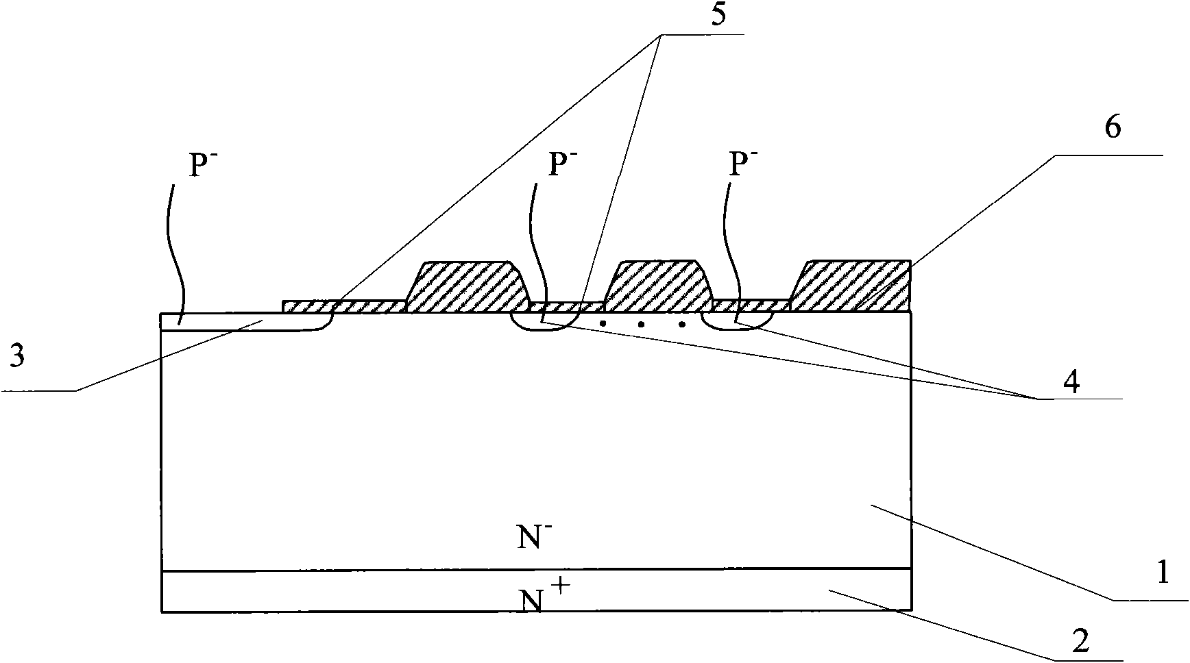
[0047] at low resistance N + Epitaxial preparation of high resistance N on substrate layer 2 - Layer 1, the high resistance N - Prepare a 1 micron thick oxide layer 6 on the layer 1, photolithography and etch the thick oxide layer 6 to form a 2 mm P - Main junction area window and 10 µm termination voltage divider ring area window; mask P with 0.5 µm photoresist - 10 microns outside the window of the main junction area, and 4 microns outside the window of the terminal pressure-dividing ring area; the energy used is 30-100 KeV, and the dose is 1×10 12 cm -2 After boron ion implantation, the photoresist is removed; boron ions are driven in at a high temperature of 1050 degrees to form P - main junction area 3 and terminal voltage divider ring area 4, P - The depth of the main junction region 3 and the terminal voltage divider ring region 4 is 1.5 microns, and the peak doping concentration of the high-concentration region of the PN junction is at 2×10 15 cm -3 , and simult...

Embodiment 2

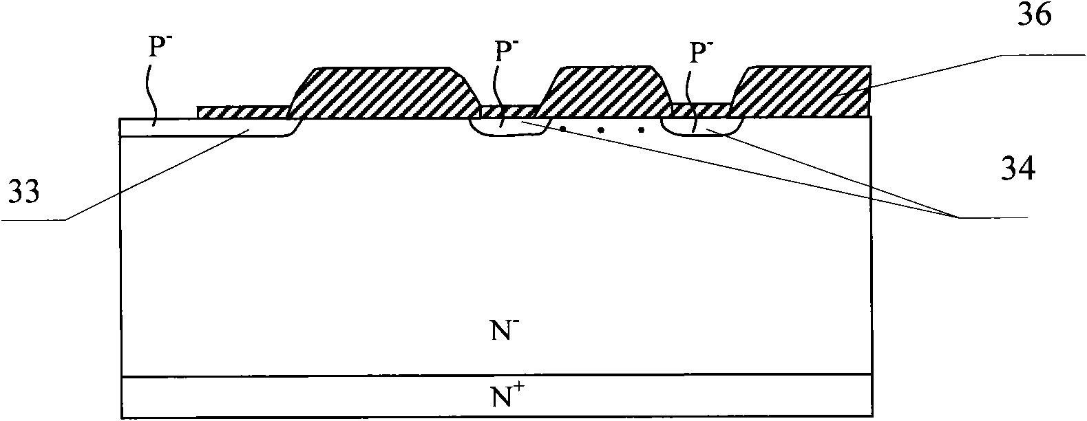
[0049] at low resistance N + Epitaxial preparation of high resistance N on substrate layer 2 - Layer 1, the high resistance N - Prepare a 1 micron thick oxide layer 6 on the layer 1, photolithography and etch the thick oxide layer 6 to form a 3.5 mm P - Main junction area window and 20 µm termination voltage divider ring area window; mask P with 0.6 µm thick photoresist - 20 microns outside the window of the main junction area and 10 microns outside the window of the terminal pressure dividing ring area; the energy is 30-100KeV, and the dose is 1×10 14 cm -2 After boron ion implantation, the photoresist is removed; boron ions are driven in at a high temperature of 1100 degrees to form P - main junction area 3 and terminal voltage divider ring area 4, P - The depth of the main junction region 3 and the terminal voltage divider ring region 4 is 2 microns, and the peak doping concentration of the high-concentration region of the PN junction is at 1×10 17 cm -3 , and simult...


PUM


Abstract

The invention provides a method for preparing a chip of a high-voltage planar fast-recovery diode (FRD). The method comprises the following steps: masking a P<-> main junction region window and a terminal potential-dividing ring region window by using photoresist; injecting low-dose boron ions and pushing the junctions at lower temperature at the same time to form low-concentration shallow PN junctions; and further masking the junction terminals of the PN junctions by using a thin oxide layer. By using the method of the invention, both the main junctions and the terminal potential-dividing rings are low-concentration shallow junctions, i.e., the effect of the anode-emitting efficiency technology can be guaranteed; after the terminals of the PN junctions are masked by the thin oxide layer, the influence on leakage caused by mobile platinum atoms can be reduced, and the high yield of the product can be guaranteed; according to the tests, the yield of the chip prepared by the method of the invention is higher than 90%; and for the total content of the mobile platinum atoms in the thin oxide layer for masking the PN junctions is more than 10 times lower than that of a thick oxide layer, the influence caused by platinum diffusion is not significant on the quality of the oxide layer, and the qualification rate is not obviously reduced after the platinum diffusion.

Description

technical field [0001] The invention relates to a manufacturing technology of a high-voltage (above 200V) power fast recovery planar diode chip, which is suitable for the manufacture of high-voltage power fast recovery diodes in discrete and integrated devices, such as chip manufacturing of high-voltage discrete power fast recovery diodes, and VDMOS phase The manufacture of an integrated power fast recovery diode chip and the manufacture of a power fast recovery diode chip integrated with an IGBT belong to the technical field of semiconductors. Background technique [0002] Power fast recovery diodes (hereinafter referred to as FRD—Fast Recovery Diode) are often used as freewheeling diodes and other purposes in power electronic circuits at the same time as three-terminal power switching devices (such as IGBTs, etc.), and are widely used in switching power supplies and pulse width modulators. (PWM), uninterruptible power supply (UPS), AC motor variable frequency speed regulat...

Claims


Application Information

Patent Timeline
Patent Type & Authority Applications(China)
IPC IPC(8): H01L21/329H01L29/861H01L29/06H01L29/36
Inventor 刘军
Owner BEIJING MXTRONICS CORP
Why Eureka
Try Eureka