Method for preparing silicon germanium on insulator (SGOI) by layer transfer technology

A technology of multi-layer materials and epitaxial materials is applied in the field of preparing silicon-germanium on insulators, and using layer transfer technology to prepare silicon-germanium-on-insulator materials, which can solve problems such as inability to prepare high-speed

Inactive Publication Date: 2010-10-20
SHANGHAI INST OF MICROSYSTEM & INFORMATION TECH CHINESE ACAD OF SCI +1
View PDF0 Cites 19 Cited by
  • Summary
  • Abstract
  • Description
  • Claims
  • Application Information

AI Technical Summary

Problems solved by technology

[0002] Manufacturing smaller-sized, higher-performance devices has always been the goal and direction of the development of the semiconductor industry. With the d

Method used


Image

  • Method for preparing silicon germanium on insulator (SGOI) by layer transfer technology
  • Method for preparing silicon germanium on insulator (SGOI) by layer transfer technology
  • Method for preparing silicon germanium on insulator (SGOI) by layer transfer technology

Examples


Embodiment 1

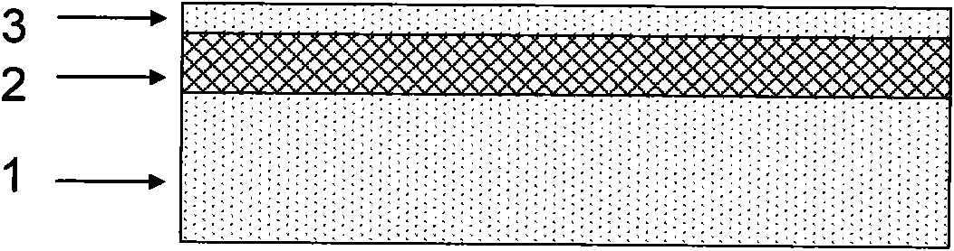
[0017] 1. Sequential epitaxy of Si on bulk silicon substrates using chemical vapor deposition 1-x Ge x 、Si epi For two different films, where 01-x Ge x Thickness of the film, making it less than the critical thickness, while ensuring Si epi thicker than Si 1-x Ge x Thickness (see attached figure 1 ).

[0018] 2. Take a piece of silicon substrate material, prepare SiO on the surface of silicon substrate by thermal oxidation, or plasma enhanced chemical vapor deposition (PECVD), or other methods 2 , SiO 2The thickness is generally 200nm ~ 1um.

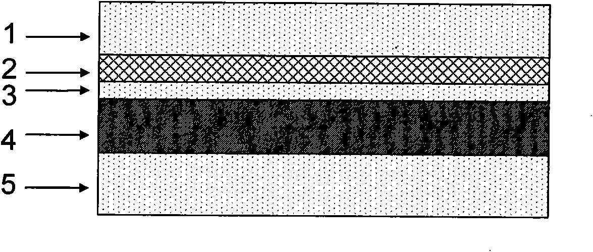
[0019] 3. Bond the material prepared in step 1 with the material prepared in step 2 (see attached figure 2 ).

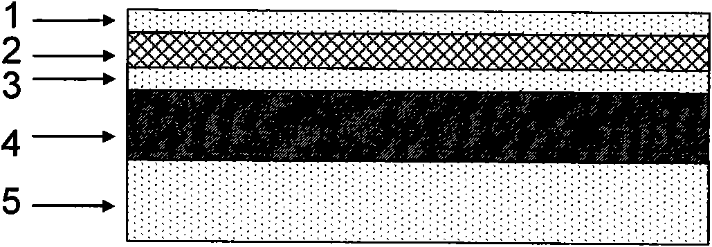
[0020] 4. By grinding, remove the material obtained in step 3 and Si 1-x Ge x Adjacent bulk Si (see attached image 3 ).

[0021] 5. A chemical solution with a high Si: SiGe etching ratio including TMAH (tetramethylammonium hydroxide) or KOH chemical solution is used as a selective etching solution to etch the re...

Embodiment 2

[0025] 1. Sequential epitaxy of Si on bulk silicon substrates using chemical vapor deposition 1-x Ge x 、Si epi Two different films, where 01-x Ge x Thickness of the film, making it less than the critical thickness, while ensuring Si epi thicker than Si 1-x Ge x Thickness (see attached figure 1 ).

[0026] 2. H + or He + Take 5×10 16 cm -2 ~1×10 17 cm -2 dose, select the appropriate energy, and inject it from the upper surface of the material prepared in step 1 into the silicon substrate layer of the epitaxial material close to the Si 1-x Ge x place for the film (see attached Figure 6 ), the preferred recommended dose is 6×10 16 cm -2 , the preferred implanted ion is H + .

[0027] 3. Take a new piece of silicon substrate material, prepare SiO on the surface of the silicon substrate by thermal oxidation, or plasma enhanced chemical vapor deposition (PECVD), or other methods 2 , SiO 2 The thickness is generally 200nm ~ 1um.

[0028] 4. Bond the material pre...


PUM

PropertyMeasurementUnit
Thicknessaaaaaaaaaa

Abstract

The invention relates to a method for preparing silicon germanium on insulator (SGOI) by the layer transfer technology, comprising the following steps: extending multiple layers of materials which are in the structure of Siepi/Si1-xGex on silicon, wherein the x is more than 0 and less than 1, and the Siepi is the upper surface of the extended material; controlling the thickness of the extended thin film which is in the structure of Si1-xGex to be less than the critical thickness so as to ensure that the extended thin film is fully strained; transferring the multiple layers of materials which are in the structure of Siepi/Si1-xGex to support materials which are in the structure of SiO2/Si by the layer transfer method to form multiple layers of materials which are in the structure of Si1-xGex/Siepi/SiO2/Si; and annealing to enable the layer of material which is in the structure of Si1-xGex to be relaxed wherein the dislocation generated in the annealing process is mainly distributed in the layer of material which is in the structure of Siepi, so that the layer of material which is in the structure of Si1-xGex keeps high lattice quality; and continuously extending a layer of thin film which is in the structure of Si on the layer of material which is in the structure of Si1-xGex by a extending method, and keeping the layer of thin film which is in the structure of Si stressed to obtain the SGOI which is in the structure of Si/Si1-xGex/Siepi/SiO2/Si.

Description

technical field [0001] The invention relates to a method for preparing silicon-germanium-on-insulator (SGOI), in particular to a method for preparing silicon-germanium-on-insulator material by using layer transfer technology. It belongs to the technical field of microelectronics and solid state electronics. Background technique [0002] Manufacturing smaller-sized, higher-performance devices has always been the goal and direction of the development of the semiconductor industry. With the development of semiconductor technology, it is no longer possible to manufacture sufficiently high-speed, low-power transistors solely relying on silicon materials. Starting from the 90nm process, strained silicon (sSi) technology and silicon-on-insulator (SOI) technology have become two powerful tools to promote Moore's Law. Now the strained silicon-on-insulator technology combined with strained silicon and SOI technology has been paid more and more attention by relevant scientific and tec...

Claims


Application Information

Patent Timeline
IPC IPC(8): H01L21/762H01L21/20
Inventor 张苗薛忠营张波魏星
Owner SHANGHAI INST OF MICROSYSTEM & INFORMATION TECH CHINESE ACAD OF SCI
Why Eureka
Try Eureka