Semiconductor device and manufacturing method

A manufacturing method and semiconductor technology, which are applied in the fields of semiconductor/solid-state device manufacturing, semiconductor devices, and semiconductor/solid-state device components, etc., can solve the problems of contact resistance and device performance attenuation, erosion, etc.

Active Publication Date: 2010-10-27
TAIWAN SEMICON MFG CO LTD
View PDF0 Cites 34 Cited by
  • Summary
  • Abstract
  • Description
  • Claims
  • Application Information

AI Technical Summary

Problems solved by technology

For example, in the process, contact openings are usually formed on the region (doped region) of the substrate (or wafer) and the gate structure thereon at the same time, but the traditional process of forming contact openings on the substrate and the gate structure will make of the gate structure (e.g. gate stack, such as polysilicon and / or gate electrodes) are corroded
This over-etching of the gate structure can lead to unwanted contact resistance and degradation of device performance

Method used


Image

  • Semiconductor device and manufacturing method
  • Semiconductor device and manufacturing method
  • Semiconductor device and manufacturing method

Examples


Embodiment Construction

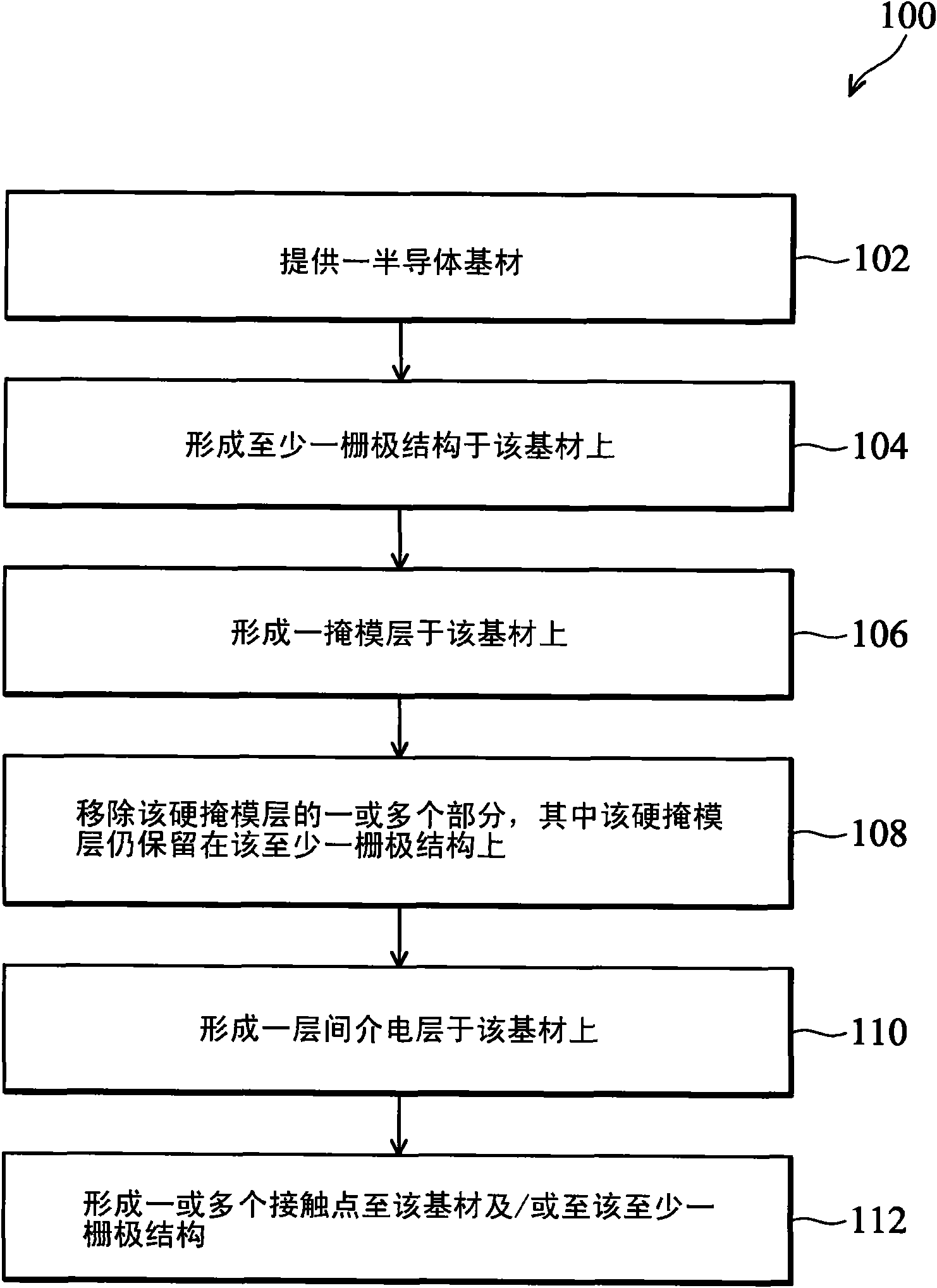
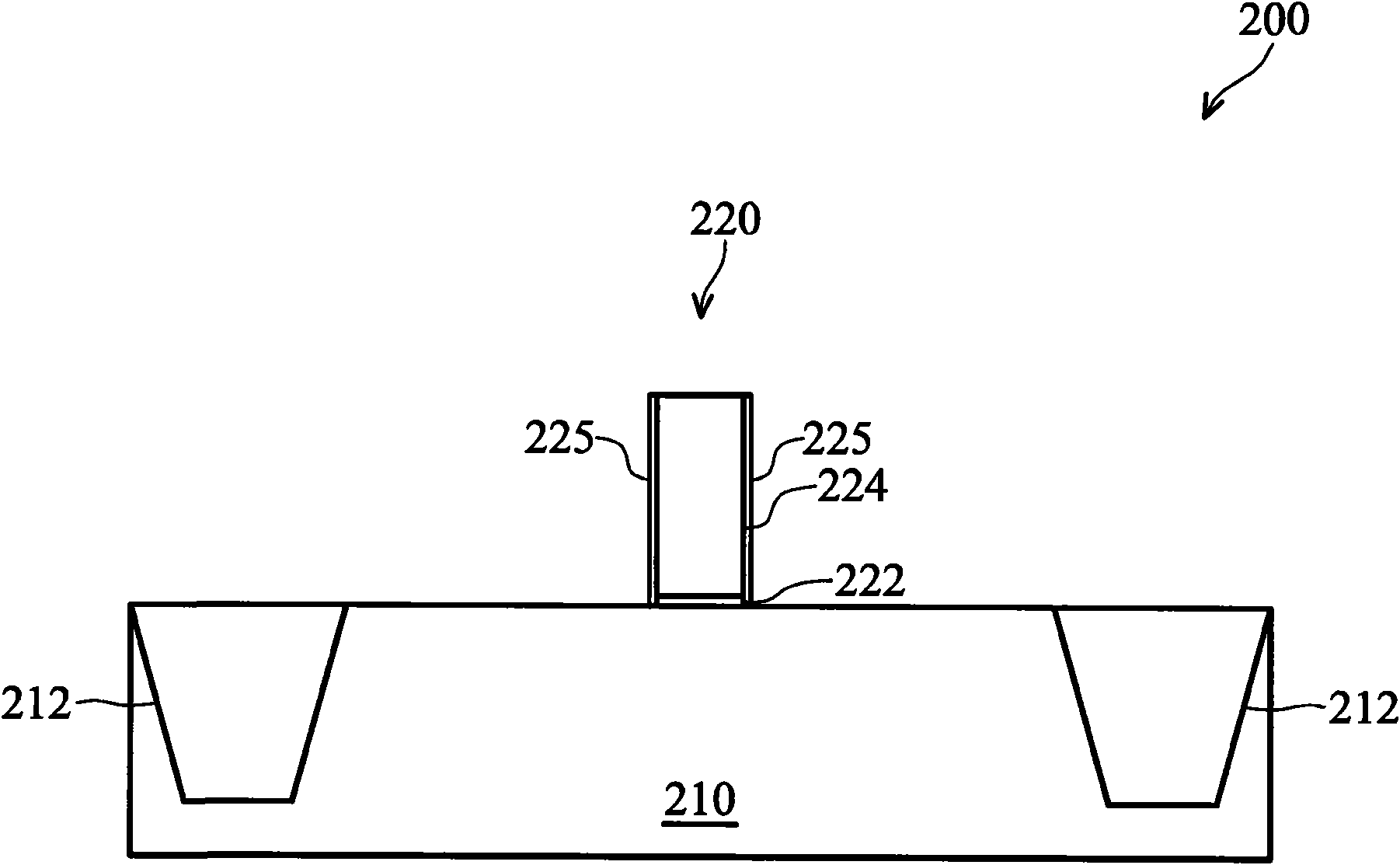
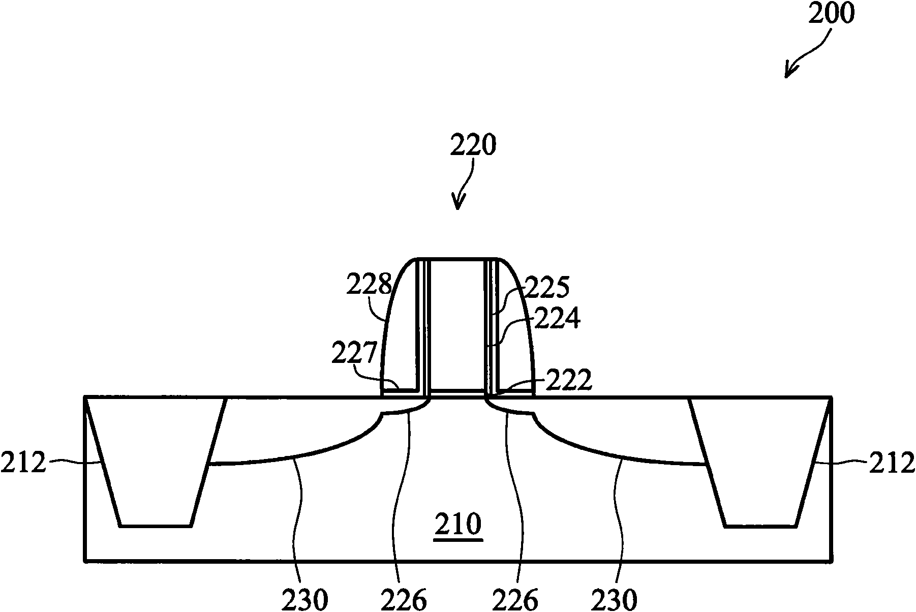
[0027] The present invention will provide many different embodiments to implement different features of the present invention. The composition and configuration of each specific embodiment will be described below to simplify the present invention. Of course, these examples are not intended to limit the present invention. For example, "above", "over", "under" or "on" a second element may include that the first element is in direct contact with the second element or that the first element is in direct contact with the second element. There are other additional elements between the second element so that the first element does not have direct contact with the second element. In addition, repeated element symbols may appear in various examples in this specification to simplify the description, but this does not mean that there is any specific relationship between the various embodiments and / or illustrations.

[0028] The following will be Figure 1 to Figure 2N For reference, t...


PUM


Abstract

A method for fabricating a semiconductor device is disclosed. The method includes providing a substrate; forming at least one gate structure over the substrate; forming a plurality of doped regions in the substrate; forming an etch stop layer over the substrate; removing a first portion of the etch stop layer, wherein a second portion of the etch stop layer remains over the plurality of doped regions; forming a hard mask layer over the substrate; removing a first portion of the hard mask layer, wherein a second portion of the hard mask layer remains over the at least one gate structure; and forming a first contact through the second portion of the hard mask layer to the at least one gate structure, and a second contact through the second portion of the etch stop layer to the plurality of doped regions.

Description

technical field [0001] The invention relates to a method for manufacturing an integrated circuit device, and in particular to a method for manufacturing an integrated circuit device that can improve device performance. Background technique [0002] The semiconductor integrated circuit (IC) industry has experienced rapid growth. Technological advances in IC materials and design have resulted in successive generations of IC production, each with smaller and more complex circuits than the previous generation. Conventional IC processing involves forming one or more contacts to various components in the IC. For example, in the process, contact openings are usually formed on the region (doped region) of the substrate (or wafer) and the gate structure thereon at the same time, but the traditional process of forming contact openings on the substrate and the gate structure will make The gate structure (eg, gate stack, such as polysilicon and / or gate electrodes) is corroded. This o...

Claims


Application Information

Patent Timeline
Patent Type & Authority Applications(China)
IPC IPC(8): H01L21/82H01L21/768H01L21/336H01L21/28H01L27/04H01L23/52
CPCH01L29/66545H01L29/4966H01L29/7833H01L29/78H01L21/823871H01L21/823828H01L21/28247H01L29/6659H01L23/485H01L29/517H01L29/6656H01L2924/0002H01L21/76897H01L21/76834H01L2924/00
Inventor 张宏迪苏培剑郑光茗陶宏远庄学理
Owner TAIWAN SEMICON MFG CO LTD
Why Eureka
Try Eureka