Method for improving efficiency of erasing floating gate

A floating gate, high efficiency technology, applied in the direction of electrical components, semiconductor/solid-state device manufacturing, circuits, etc., can solve the problem of low erasing efficiency of floating gates, to increase erasing efficiency, increase erasing efficiency, reduce erasing The effect of voltage

Active Publication Date: 2010-11-10
SEMICONDUCTOR MANUFACTURING INTERNATIONAL (BEIJING) CORP
View PDF0 Cites 9 Cited by
  • Summary
  • Abstract
  • Description
  • Claims
  • Application Information

AI Technical Summary

Problems solved by technology

[0009] In view of this, the technical problem solved by the present invention is: the problem that the erasing efficiency of the existing floating gate is low

Method used


Image

  • Method for improving efficiency of erasing floating gate
  • Method for improving efficiency of erasing floating gate
  • Method for improving efficiency of erasing floating gate

Examples


Embodiment Construction

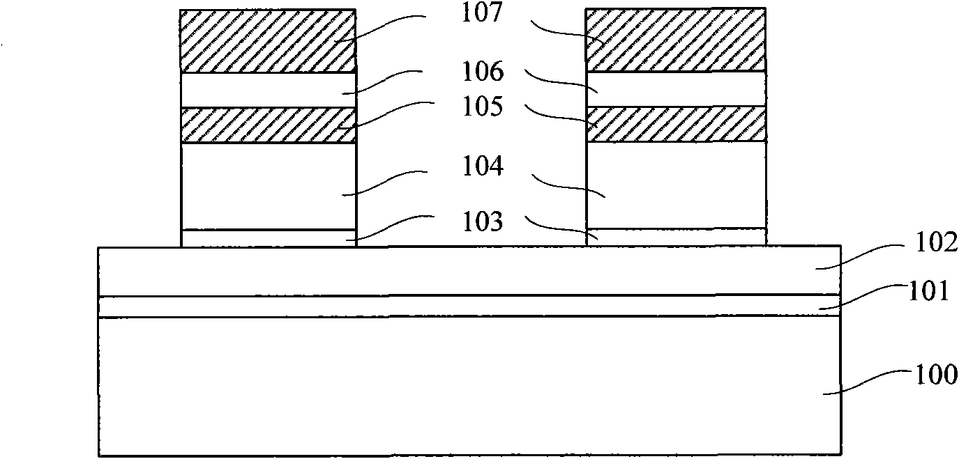
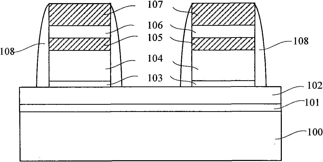
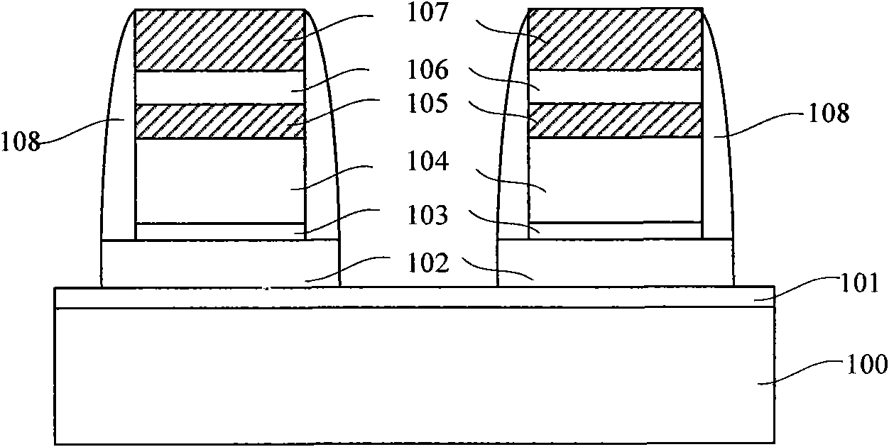
[0029] In order to make the object, technical solution, and advantages of the present invention clearer, the present invention will be further described in detail below with reference to the accompanying drawings and examples.

[0030] In order to make the above objects, features and advantages of the present invention more comprehensible, specific implementations of the present invention will be described in detail below in conjunction with the accompanying drawings. Of course, the present invention is not limited to this specific embodiment, and general replacements known to those skilled in the art undoubtedly fall within the protection scope of the present invention.

[0031] The present invention has been described in detail using schematic diagrams. When describing the embodiments of the present invention in detail, for the convenience of explanation, the schematic diagram showing the structure will not be partially enlarged according to the general scale, which should no...


PUM


Abstract

The invention discloses a method for improving the efficiency of erasing a floating gate, which comprises the following steps: sequentially forming a floating gate (FG) oxide layer, a FG polycrystalline silicon layer, an oxide layer-nitride layer-oxide layer (ONO) dielectric layer, a control gate (CG) polycrystalline silicon layer, a CG silicon nitride layer, a CG silicon oxide layer and a CG silicon nitride hard mask layer on a semiconductor substrate; coating photoresist on the CG silicon nitride hard mask layer, and patterning the photoresist; taking the patterned photoresist as a mask, and sequentially etching the CG silicon nitride hard mask layer, the CG silicon oxide layer, the CG silicon nitride layer, the CG polycrystalline silicon layer and the ONO dielectric layer to form two CGs; forming a CG side wall layer at two sides of each CG; forming a sacrificial layer at the outside of each CG side wall layer; taking the CG side wall layers, the sacrificial layer and the CG as masks, and etching the FG polycrystalline silicon layer to form FG; removing the sacrificial layer; and sequentially forming the oxide layer and depositing the polycrystalline silicon film outside the CG side wall layer and the FG, and finally forming the erasing gate EG by the polycrystalline silicon film. The method can effectively improve the efficiency of erasing the floating gate.

Description

technical field [0001] The invention relates to the technical field of semiconductor manufacturing, in particular to a method for improving the erasing efficiency of a floating gate. Background technique [0002] At present, in the development of 70nm split-gate flash (Split-Gate Flash) technology, the erasing efficiency of the floating gate (Floating Gate, FG) in the memory cell area is relatively low, such as having an erasing voltage of 13 volts and an erasing time of 5 seconds. except time. Improving erasing efficiency has increasingly become a key technology in the high-end split-gate flash memory manufacturing process. [0003] Figure 1a to Figure 1d A schematic cross-sectional view of a manufacturing process of a memory cell region in the prior art is shown. [0004] First, if Figure 1a As shown, a FG oxide layer 101, a FG polysilicon layer 102, an oxide layer-nitride layer-oxide layer (ONO) dielectric layer 103, a control gate (Control Gate, CG) polysilicon laye...

Claims


Application Information

Patent Timeline
Patent Type & Authority Applications(China)
IPC IPC(8): H01L21/283H01L21/31H01L21/8247
Inventor 李勇刘艳周儒领黄淇生詹奕鹏
Owner SEMICONDUCTOR MANUFACTURING INTERNATIONAL (BEIJING) CORP
Why Eureka
Try Eureka