Dual-gate field-effect transistor

A field-effect transistor, double-gate technology, applied in semiconductor devices, electrical components, circuits, etc., can solve the problem of unreported semiconductor manufacturing processes, and achieve the advantages of avoiding secondary effects, small sub-threshold swings, and reducing energy consumption. Effect

Active Publication Date: 2010-11-24
SEMICON MFG INT (SHANGHAI) CORP
View PDF0 Cites 11 Cited by
  • Summary
  • Abstract
  • Description
  • Claims
  • Application Information

AI Technical Summary

Problems solved by technology

[0008] At present, the concept of green transistors is only in the research of theoretical models, but there is no report on the actual manufacturing process applied to semiconductors.

Method used


Image

  • Dual-gate field-effect transistor
  • Dual-gate field-effect transistor
  • Dual-gate field-effect transistor

Examples


Embodiment Construction

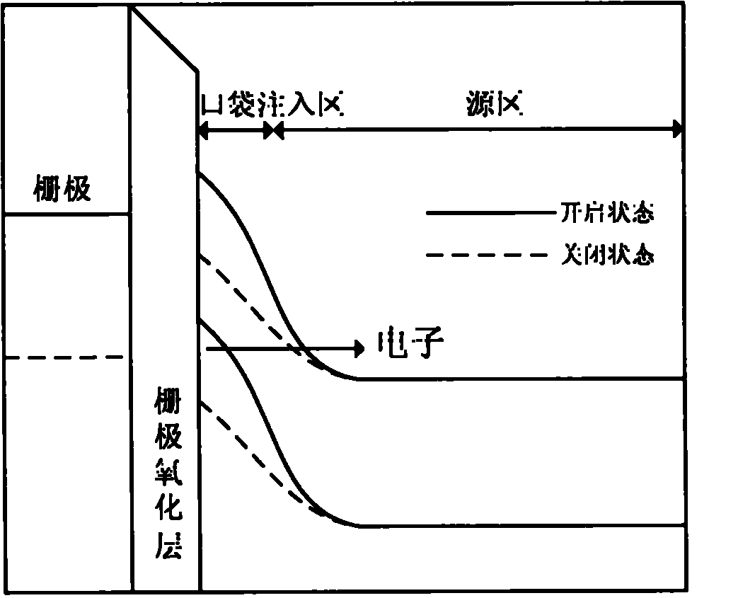
[0043] It is known from the prior art that the green transistor has lower energy consumption and stable device characteristics in a small size, which meets the low energy consumption requirement of VDD scaling down. On this basis, the present invention provides a new dual-gate pole field effect transistor.

[0044] The specific embodiments of the present invention will be described in detail below in conjunction with the accompanying drawings.

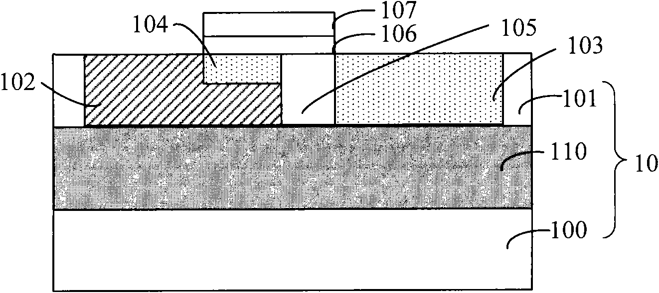
[0045] Figure 4 It is a schematic cross-sectional structure diagram of the double gate field effect transistor of the first embodiment provided by the present invention. include:

[0046] a device layer 200 having opposing first and second surfaces;

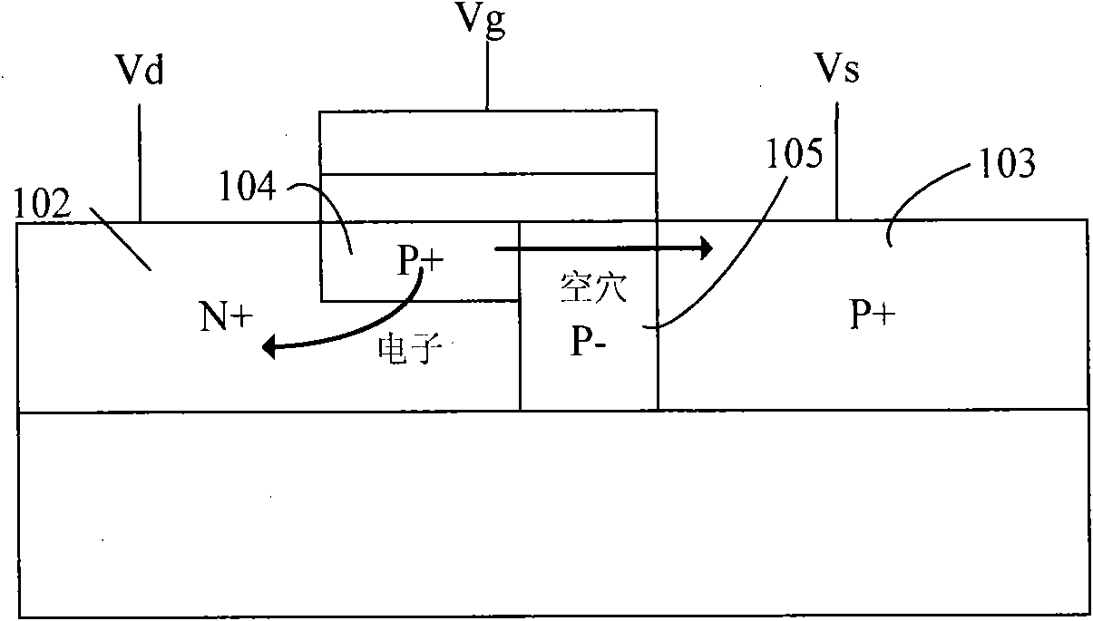
[0047] A source 1 and a drain 2 that are isolated from each other and have different conductivity types in the device layer 200;

[0048] a channel region between source 1 and drain 2;

[0049] The channel region sequentially includes a first pocket injection region 3a, a source con...


PUM


Abstract

The invention provides a dual-gate field-effect transistor which comprises a device layer, a source, a drain, a channel region positioned between the source and the drain, a first gate structure and a second gate structure, wherein the device layer comprises a first surface and a second surface which are opposite to each other; the source and the drain are positioned in the device layer, isolated mutually and have different conduction types; the channel region sequentially comprises a first pocket injection region, a source connection region and a second pocket injection region from the first surface to the second surface of the device layer, the first and the second pocket injection regions are electrically connected with the drain, and the source connection region is electrically connected with the source; the first gate structure is positioned on the first surface of the device layer and corresponds to the position of the first pocket injection region; and the second gate structure is positioned on the second surface of the device layer and corresponds to the position of the second pocket injection region. The dual-gate field-effect transistor has high response speed and sensitive switching property, and can meet the demand of reducing the energy consumption after scaling down a device under small size and avoid the production of a series of secondary effects.

Description

technical field [0001] The invention relates to a field effect transistor, in particular to a double gate field effect transistor. Background technique [0002] In the development process of semiconductor VLSI, under the guidance of scaling of CMOS devices, the density and performance of transistors have been continuously and systematically increased following Moore's law. However, when the semiconductor industry develops to the 45nm node or smaller, the power consumption and power consumption density of chips have gradually become a problem that needs to be solved urgently. The power supply voltage has maintained 5V as the standard for all levels of technology for a long time. Therefore, scaling down the external voltage source (VDD-scaling) has increasingly become a bottleneck restricting the development of metal oxide field effect transistors (MOSFETs). [0003] At present, it has been proposed that the use of gate bias in metal-oxide field-effect transistors can induce...

Claims


Application Information

Patent Timeline
Patent Type & Authority Applications(China)
IPC IPC(8): H01L29/78
Inventor 肖德元季明华吴汉明
Owner SEMICON MFG INT (SHANGHAI) CORP
Why Eureka
Try Eureka