Method for obtaining vertical channel high-voltage super junction-semiconductor device

A super junction and semiconductor technology, used in semiconductor/solid-state device manufacturing, electrical components, circuits, etc., can solve the problems of high cost, complex process, poor stability and repeatability of mass production, etc., achieve high aspect ratio, reduce Effects of diffusion and low resistance resistance

Active Publication Date: 2010-12-01
SHANGHAI HUAHONG GRACE SEMICON MFG CORP
View PDF0 Cites 7 Cited by
  • Summary
  • Abstract
  • Description
  • Claims
  • Application Information

AI Technical Summary

Problems solved by technology

The first method is not only complicated in process, high in cost, but also difficult to realize; for example, a general 600V device requires 5-7 epitaxial growth-lithography-implantation times. After multiple epitaxial growths, the alignment marks required for lithography are often Because the deformation cannot be identified, it is necessary to make a new alignment mark through an additional process after 2-3 epitaxial growths
In the second method, oblique implantation cannot be used in mass production due to poor stability and repeatability, and P-type polysilicon with the required impurity concentration has not been realized in the process so far, so the P-type epitaxial filling process has received great attention.
Compared with the vertical device, the unit area of ​​the planar device is large, so the specific resistance of the planar device is relatively large

Method used


Image

  • Method for obtaining vertical channel high-voltage super junction-semiconductor device
  • Method for obtaining vertical channel high-voltage super junction-semiconductor device
  • Method for obtaining vertical channel high-voltage super junction-semiconductor device

Examples


Embodiment Construction

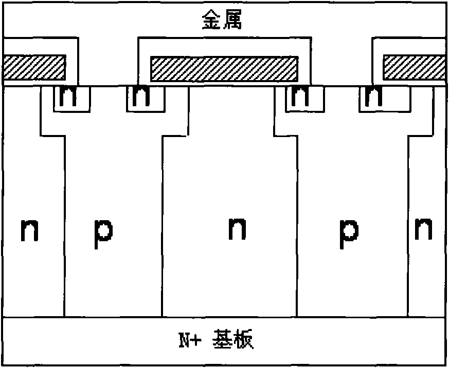
[0029] see Figure 2-8 As shown, the method for obtaining a vertical channel high-voltage super junction semiconductor device in the present invention includes the following process steps:

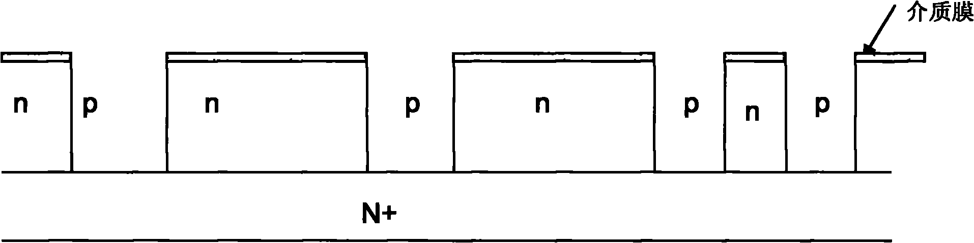
[0030] Step 1: Perform the first N-type epitaxial growth on the N+ substrate, and form a layer of dielectric film on the N-type epitaxial layer.

[0031] Step 2: Etching the N-type epitaxial layer, forming a groove with a certain aspect ratio on the N-type epitaxial layer to penetrate to the N+ substrate (see figure 2 shown). The etching method can adopt various known existing technologies. The trenches with a certain aspect ratio may be trenches with an aspect ratio greater than or equal to 4:1.

[0032] Step three, see image 3 As shown, the trench is filled with a P-type epitaxial layer.

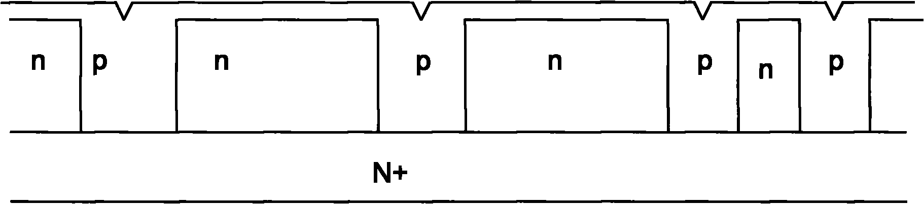
[0033] Step 4, using chemical mechanical grinding to obtain a structure in which flat N-type pillars and P-type pillars appear alternately (combined Figure 4 shown).

[0034] Step 5. Perform ...


PUM


Abstract

The invention discloses a method for obtaining a vertical channel high-voltage super junction-semiconductor device, comprising the following steps of: firstly, carrying out first N-type epitaxial growth on an N+ base plate; secondly, etching an N-type epitaxial layer and forming a groove which has a certain depth-width ratio and passes through the N+ base plate on the N-type epitaxial layer ; thirdly, filling a P-type epitaxial layer into the groove; fourthly, obtaining a smooth alternating appearing structure of an N-type pillar and a P-type pillar by using a chemical machine to grind; fifthly, carrying out second N-type epitaxial growth on the alternating appearing structure of the N-type pillar and the P-type pillar formed in the fourth step, then, obtaining a smooth alternating appearing structure with a higher depth-width ratio of the P-type groove of the N-type pillar and the P-type pillar by repeatedly carrying out the second step, the third step and the fourth step until the thickness of the N-type epitaxial layer achieves a requirement of using the device to block voltage. The invention can effectively reduce the proportion of the P-type pillar and specific resistance without increasing the process difficulty.

Description

technical field [0001] The invention relates to a manufacturing process method of a semiconductor integrated circuit, in particular to a method for obtaining a vertical channel high-voltage super junction semiconductor device. Background technique [0002] The super junction MOSFET (metal-oxide-semiconductor field-effect transistor) adopts a new voltage-resistant layer structure, using a series of alternately arranged P-type and N-type semiconductor thin layers (semiconductor thin layers or called pillars ), the P-type and N-type regions are depleted in the off state and at a lower voltage to achieve mutual compensation of charges; thus enabling the N-type region to achieve a high breakdown voltage at a high doping concentration while obtaining a low on-resistance , breaking the theoretical limit of traditional power MOSFETs. Therefore, this new voltage-resistant layer structure has received more and more attention in high-voltage devices. [0003] The new fabrication meth...

Claims


Application Information

Patent Timeline
Patent Type & Authority Applications(China)
IPC IPC(8): H01L21/337
Inventor 肖胜安
Owner SHANGHAI HUAHONG GRACE SEMICON MFG CORP
Why Eureka
Try Eureka