High voltage low resistance MOSFET device and its manufacture method

A device and semiconductor technology, applied in the field of metal oxide semiconductor field effect transistors, can solve the problems of increasing on-resistance, hindering the flow of channel electrons, increasing on-resistance, etc., to reduce on-resistance and improve device performance. performance, the effect of eliminating channel bend structure

Active Publication Date: 2010-12-01
CHENGDU MONOLITHIC POWER SYST
View PDF5 Cites 10 Cited by
  • Summary
  • Abstract
  • Description
  • Claims
  • Application Information

AI Technical Summary

Problems solved by technology

In this way, the step will sit above the channel of the NMOS, which is in the figure 1 The top is the dotted line area where the P well and the gate overlap. This step makes the c

Method used


Image

  • High voltage low resistance MOSFET device and its manufacture method
  • High voltage low resistance MOSFET device and its manufacture method
  • High voltage low resistance MOSFET device and its manufacture method

Examples


Embodiment Construction

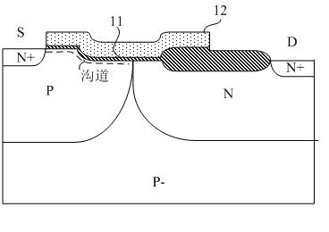
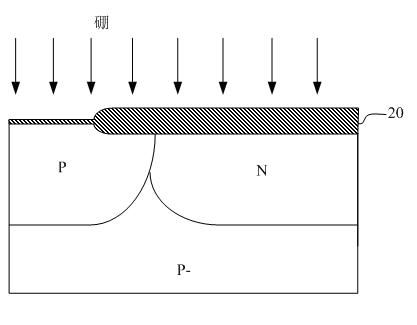
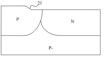
[0020] Figure 3A An embodiment of a high-voltage lateral N-type MOSFET (NMOS) 30 of the present invention is shown, wherein the gate region 31 of the high-voltage NMOS 30 is relatively short compared with the prior art, the gate region 31 and the semiconductor step 21 do not overlap, and the semiconductor step 21 is located outside the edge of the gate region 31, so that the channel region has a horizontal structure. Such as Figure 3A As shown, in the illustrated embodiment, the high voltage NMOS 30 includes a substrate 300 , a drain region D, a source region S and a gate region G. The illustrated substrate 300 is P-type doped. The drain region D and the source region S are formed on the P-type substrate 300 and are respectively located on two sides of the gate region G. From the upper surface of the P-type substrate 300, an N well 301 is formed on the drain region D side. A high concentration N+ drain contact region 308 is contained in the N well 301 . In another embodi...


PUM


Abstract

The invention discloses a high voltage NMOS using the tagma double-times doping way, wherein the second time doping is performed by the self-alignment and the step phenomenon in the channel is eliminated and the device performance is increased.

Description

technical field [0001] The invention relates to a metal oxide semiconductor field effect transistor (MOSFET), in particular to a low-resistance high-voltage N-type MOSFET (NMOS). Background technique [0002] For lateral high-voltage MOSFETs fabricated in BiCMOS or BCDMOS processes, low on-resistance and high voltage are the two main design factors. figure 1 A conventional lateral type high voltage NMOS is shown. Figure 2A , 2B show two process steps in the manufacturing process used to describe the structural characteristics of the traditional high-voltage N-type MOSFET (NMOS). Such as figure 1 As shown, the high-voltage NMOS includes a P-type substrate with a P-well and an N-well on the P-type substrate. The NMOS further includes a gate G composed of an oxide layer 11 and a polysilicon layer 12 , an N+ source region S and an N+ drain region D. Such as Figure 2A As shown, in the conventional process, the P-well is formed by doping the N-well oxide layer 20 as a barri...

Claims


Application Information

Patent Timeline
IPC IPC(8): H01L29/78H01L29/10H01L29/36H01L21/336H01L21/22
CPCH01L29/66659H01L29/42356H01L29/1083H01L29/0657H01L29/0847H01L29/42368H01L29/7835
Inventor 吉扬永
Owner CHENGDU MONOLITHIC POWER SYST
Why Eureka
Try Eureka