Process for preparing selective emitter solar crystalline silicon solar cell
A solar cell and preparation process technology, applied in the field of solar cells, can solve problems such as high cost, relatively high equipment requirements, complex process, etc., and achieve the effects of good repeatability, high process controllability, and convenience for mass production
- Summary
- Abstract
- Description
- Claims
- Application Information
AI Technical Summary
Problems solved by technology
Method used
Image

Examples
Embodiment 1
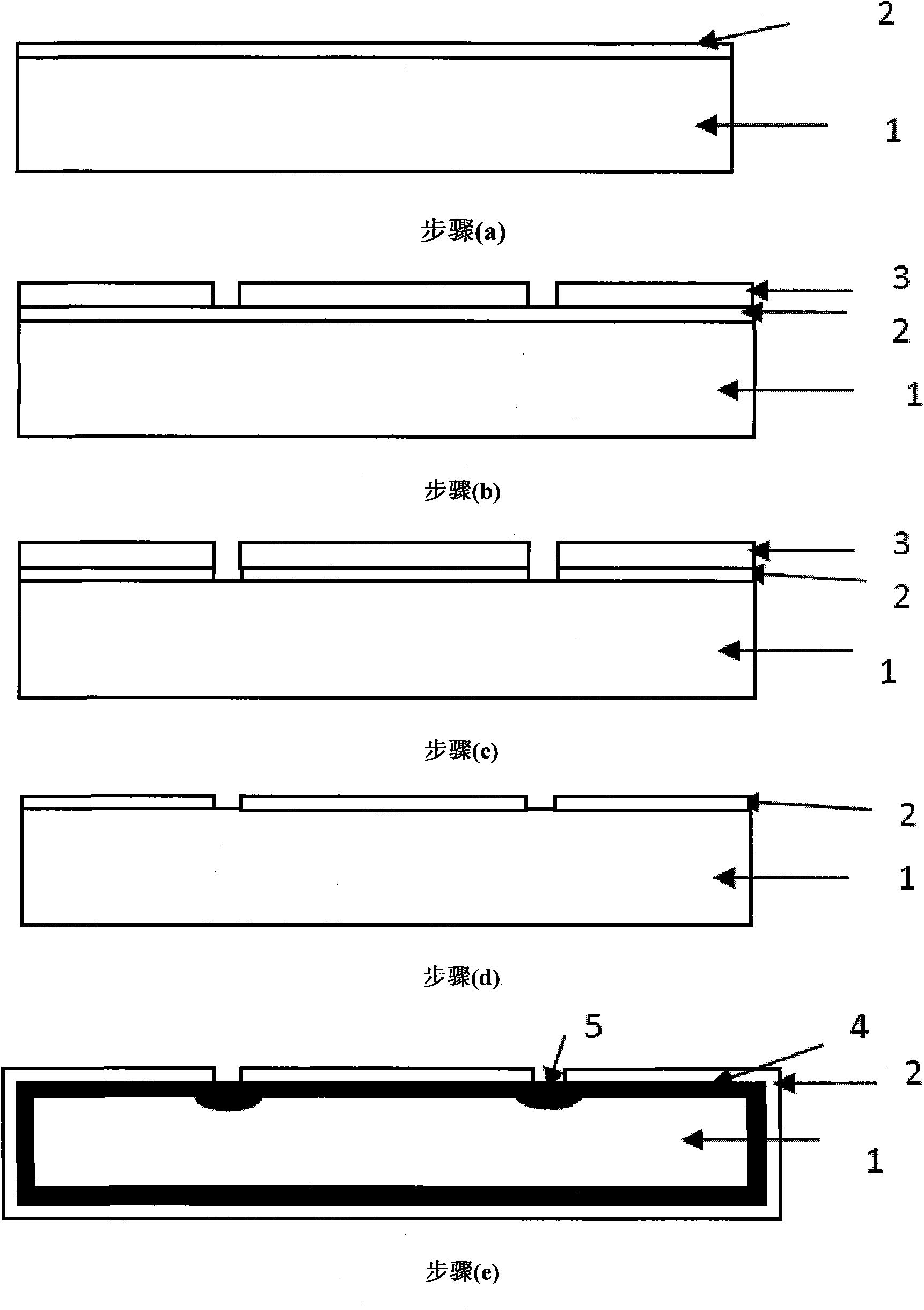
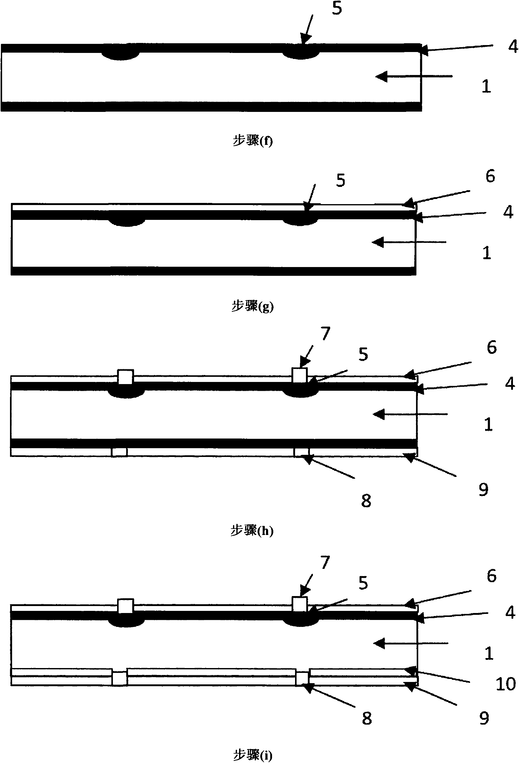
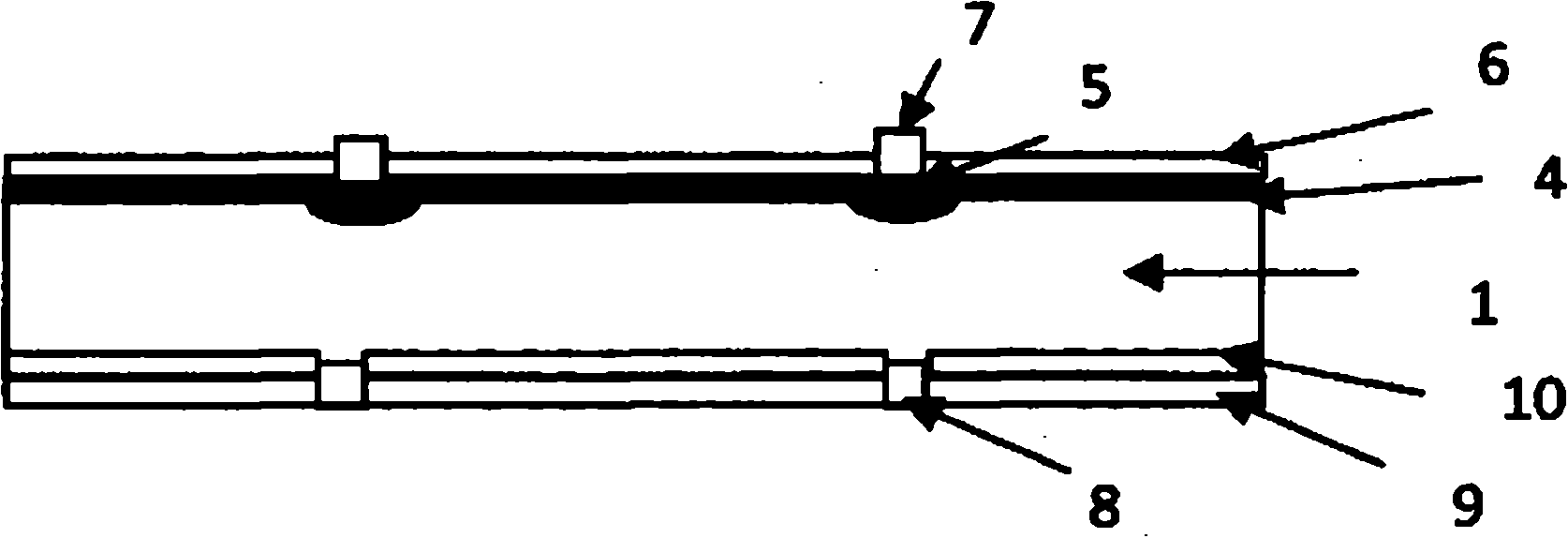
[0040] The preparation process of the selective emitter crystalline silicon solar cell provided in this embodiment includes the following steps:
[0041] (a) Select a silicon wafer, remove the damaged layer, clean it with an acid-base solution, prepare a suede structure on the surface, and coat a layer of amorphous silicon film on the surface of the silicon wafer to be diffused. The amorphous silicon film is intrinsic amorphous silicon Thin film, the thickness of which is 1-1000nm, and the preparation method of amorphous silicon thin film is chemical vapor deposition or physical vapor deposition, etc.;
[0042] The intrinsic amorphous silicon film is used as a semi-barrier layer for diffusion, which cannot completely block the diffusion of the dopant source, but will effectively reduce the doping depth and doping amount entering the crystalline silicon; in the process of selective diffusion, due to the The blocking of the amorphous silicon film can simultaneously achieve high ...
Embodiment 2
[0052] The preparation process of the selective emitter crystalline silicon solar cell provided in this embodiment includes the following steps:
[0053](a) Select a silicon wafer, remove the damaged layer, clean it with an acid-base solution, prepare a suede structure on the surface, and coat a layer of amorphous silicon film on the surface of the silicon wafer to be diffused. The amorphous silicon film is intrinsic amorphous silicon Thin film, the thickness of which is 1-1000nm, and the preparation method of amorphous silicon thin film is chemical vapor deposition or physical vapor deposition, etc.;
[0054] The intrinsic amorphous silicon film is used as a semi-barrier layer for diffusion, which cannot completely block the diffusion of the dopant source, but will effectively reduce the doping depth and doping amount entering the crystalline silicon; in the process of selective diffusion, due to the The blocking of the amorphous silicon film can simultaneously achieve high a...
Embodiment 3
[0064] The preparation process of the selective emitter crystalline silicon solar cell provided in this embodiment includes the following steps:
[0065] (a) Select a silicon wafer, remove the damaged layer, clean it with an acid-base solution, prepare a suede structure on the surface, and coat a layer of amorphous silicon film on the surface of the silicon wafer to be diffused. The amorphous silicon film is intrinsic amorphous silicon Thin film, the thickness of which is 1-1000nm, and the preparation method of amorphous silicon thin film is chemical vapor deposition or physical vapor deposition, etc.;
[0066] The intrinsic amorphous silicon film is used as a semi-barrier layer for diffusion, which cannot completely block the diffusion of the dopant source, but will effectively reduce the doping depth and doping amount entering the crystalline silicon; in the process of selective diffusion, due to the The blocking of the amorphous silicon film can simultaneously achieve high ...
PUM
 Abstract
Description
Claims
Application Information
 - R&D
- Intellectual Property
- Life Sciences
- Materials
- Tech Scout
- Unparalleled Data Quality
- Higher Quality Content
- 60% Fewer Hallucinations
Browse by: Latest US Patents, China's latest patents, Technical Efficacy Thesaurus, Application Domain, Technology Topic, Popular Technical Reports.
© 2025 PatSnap. All rights reserved.Legal|Privacy policy|Modern Slavery Act Transparency Statement|Sitemap|About US| Contact US: help@patsnap.com