Composite photonic structure element, surface emitting laser using the composite photonic structure element, wavelength conversion element, and laser processing device using the wavelength conversion element

A wavelength conversion and component technology, applied in instruments, optics, nano-optics, etc., can solve problems such as disordered position and orientation relationship, difficult beam orientation or polarization plane control, etc.

Inactive Publication Date: 2010-12-15
PUBLIC UNIVERSITY CORPORATION OSAKA CITY UNIVERSITY +2
View PDF1 Cites 3 Cited by
  • Summary
  • Abstract
  • Description
  • Claims
  • Application Information

AI Technical Summary

Problems solved by technology

In addition, the polarization plane of the light must be aligned with an intermediate direction, and since the laser beam cannot be incident at a right angle to the crystal plane in most cases, it is difficult to control the orientation or polarization plane of the beam
Even if it is temporarily adjusted to the optimal orientation, since it is used for laser processing, the laser energy is large and the optical components are heated strongly, and it is located in a working environment with a lot of vibration and noise. Confused

Method used


Image

  • Composite photonic structure element, surface emitting laser using the composite photonic structure element, wavelength conversion element, and laser processing device using the wavelength conversion element
  • Composite photonic structure element, surface emitting laser using the composite photonic structure element, wavelength conversion element, and laser processing device using the wavelength conversion element
  • Composite photonic structure element, surface emitting laser using the composite photonic structure element, wavelength conversion element, and laser processing device using the wavelength conversion element

Examples


no. 1 Embodiment approach

[0120] First, a first embodiment of the present invention will be described. Hereinafter, in order to understand the present invention, it will be described in order starting with an easy-to-understand model.

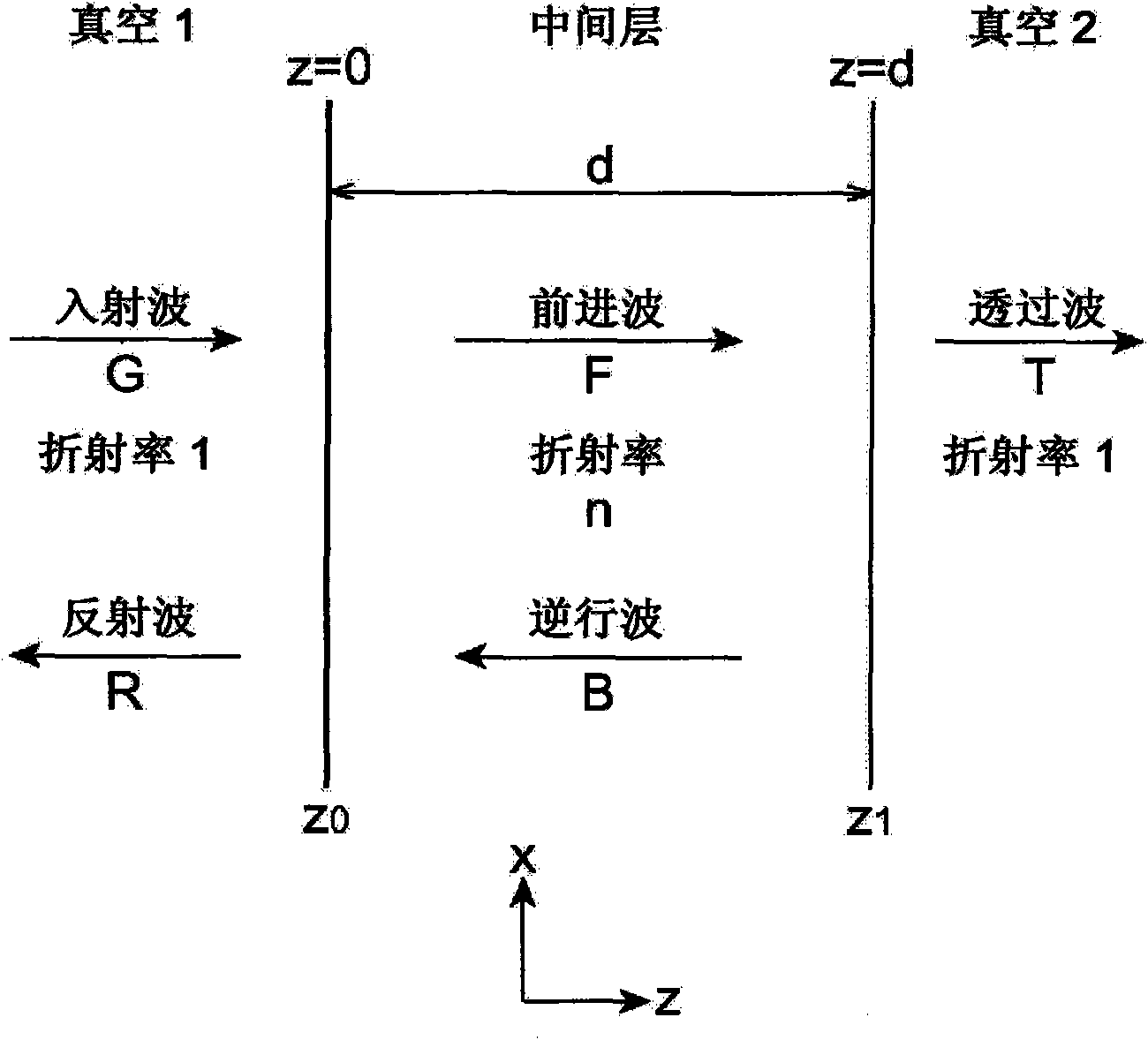
[0121] [1. Electric field of monolayer film]

[0122] First, the relationship of the steady-state electric field generated in the case of a monolayer film was investigated. Such as figure 1 As shown, it is formed in the form of vacuum 1, intermediate layer, and vacuum 2. Let the traveling direction of light be the z-axis, the upward coordinate be the x-axis, and the vertically upward coordinate with respect to the paper surface be the y-axis. Although oblique incidence is possible, here, for simplicity, the layers are arranged in the z direction so that the interface between the layers is the xy plane. Due to the use of plane waves, the electric field only has the x component E x . Since there is no distortion, only E exists in all layers x . Since it is the sam...

Embodiment 1

[0284] Next, Example 1 of the first embodiment of the present invention will be described.

[0285] If the embodiment of the present invention is explained from the beginning, it is difficult to fully understand its effect. Therefore, the case of a single-layer film and the case of a photonic crystal will be described in advance, and then the composite photonic crystal of the photon + resonator of the present invention will be described. Subsequently, a comparative example using a resonator sandwiched on both sides of a GaAs monolayer film will be described.

[0286] [1. In case of GaAs monolayer film ( Figure 4 )]

[0287] Figure 4 It shows the change in the intensity of the second harmonic when the film thickness L of the GaAs single-layer film is changed. The horizontal axis represents the film thickness L (nm). The vertical axis is the intensity of the second harmonic. The fundamental wave is infrared light with a wavelength of 1864 nm (161 THz) having energy of 0....

Embodiment 2

[0342] Next, Example 2 of the first embodiment of the present invention will be described.

[0343] [Embodiment 2: Changes in the second harmonic when the total number of layers is increased ( Figure 15 )]

[0344] On both sides of the GaAs / AlGaAs basic photonic crystal composed of 40 periods, a photonic crystal or resonator (reflector) of the same combination is further added, and the fundamental wave is vertically incident from one end, and the second harmonic generated on the opposite side is investigated. increase and decrease.

[0345] [1. Basic photonic crystal (GaAs / AlGaAs)]

[0346] The active layer is GaAs, the inactive layer is Al 0.79 Ga 0.21 As. The number of layers is 40 layers, forming 40 cycles.

[0347] Al 0.79 Ga 0.21 As dielectric constant 0.9×(light energy)+8.3

[0348] GaAs film thickness = 140nm,

[0349] Al 0.79 Ga 0.21 As film thickness = 147.5nm

[0350] 40 period film thickness = 11500nm

[0351] The intensity of the second harmonic is 1...


PUM

PropertyMeasurementUnit
wavelengthaaaaaaaaaa
thicknessaaaaaaaaaa

Abstract

A composite photonic structure element includes a photonic crystal and a multi-layer film. The photonic crystal is formed by alternately laying an active layer having a nonlinear effect for converting a fundamental wave into a second higher harmonic and an inactive layer having no nonlinear effect, so that the energy of the fundamental wave coincides with the photonic band gap end. The multi-layer film is formed by layering a plurality of sets of two types of thin films having different refractive indexes so as to reflect the fundamental wave. The multi-layer film is connected to both ends of the photonic crystal. The fundamental wave comes into one of the end faces and the fundamental wave is reciprocally reflected between resonators having a multi-layer film so that the intensity of the fundamental wave in the photonic crystal is increased. The fundamental wave is converted into a second higher harmonic in the active layer and the second higher harmonic is extracted outside from the other end face.

Description

technical field [0001] The present invention relates to a compound photon structural element that converts the wavelength of laser light into a second harmonic by using nonlinear optical effects to generate a third nonlinear signal, a surface emitting laser using the compound photon structural element, a wavelength conversion element, and a Laser processing device for transforming elements. The technique of converting the fundamental wave (wavelength 1.06 μm) of YAG laser to the second harmonic wave (532 nm) using a nonlinear element for the purpose of laser processing has been widely used. This is a laser processing device composed of a laser that generates a fundamental wave, a wavelength conversion element that converts the fundamental wave into a second harmonic, and an optical system that condenses the second harmonic and irradiates the target. Materials that are transparent to the fundamental and opaque to the second harmonic can be processed by the second harmonic. Th...

Claims


Application Information

Patent Timeline
Patent Type & Authority Applications(China)
IPC IPC(8): G02F1/37
CPCG02F1/3775G02F1/017G02F2203/15G02F2202/32B82Y20/00
Inventor 石原一葛原聪江畑惠司栗巢贤一
Owner PUBLIC UNIVERSITY CORPORATION OSAKA CITY UNIVERSITY
Why Eureka
Try Eureka