

Light-emitting diode packaging structure and packaging method thereof
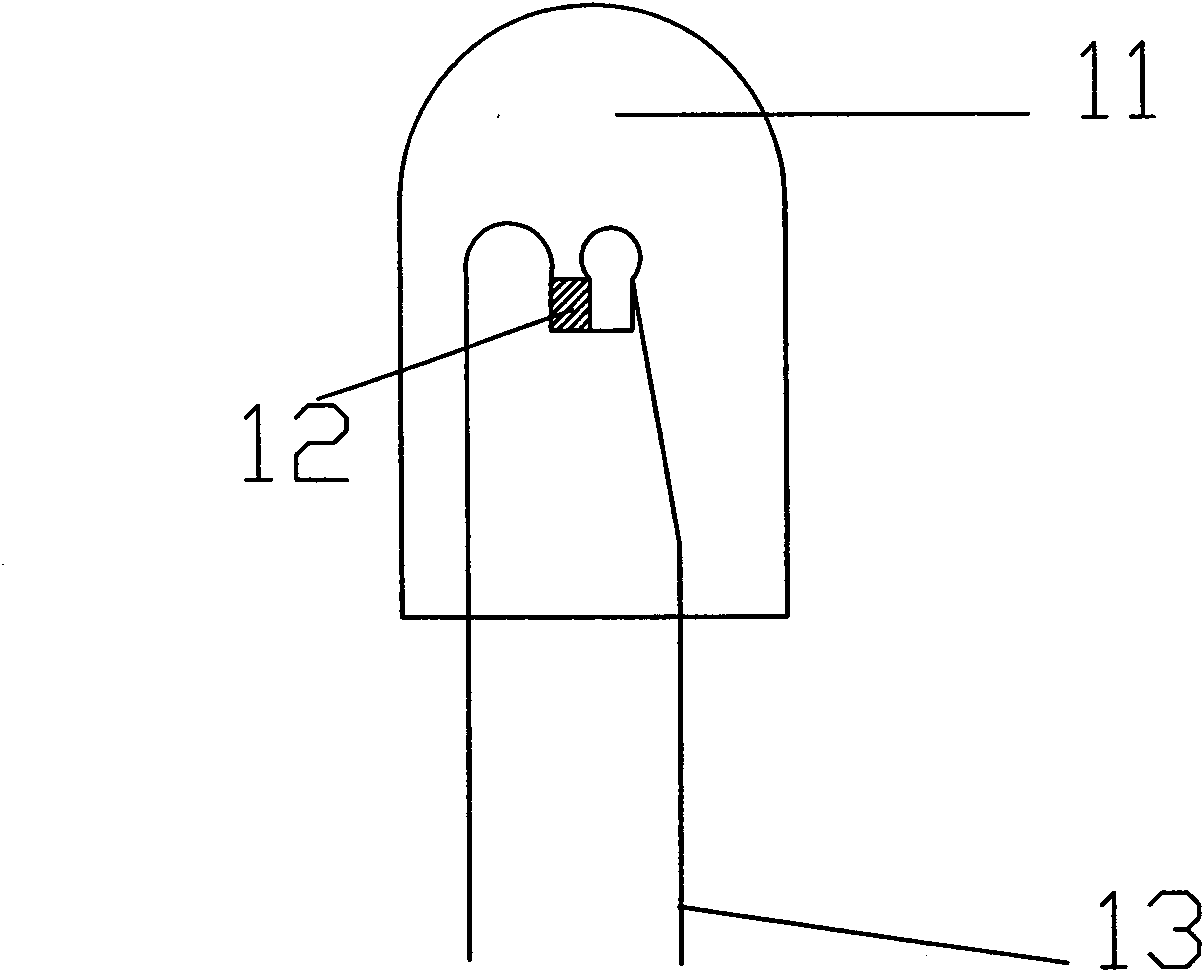
A technology of light emitting diodes and packaging structures, applied in the directions of semiconductor devices, electrical components, circuits, etc., can solve the problems of small heat conduction area of the metal bracket 13, difficult to achieve heat dissipation effect, poor thermal conductivity, etc., and achieves material saving and simple structure. , the effect of strong adaptability
- Summary
- Abstract
- Description
- Claims
- Application Information
AI Technical Summary
Problems solved by technology
Method used
Image

Examples
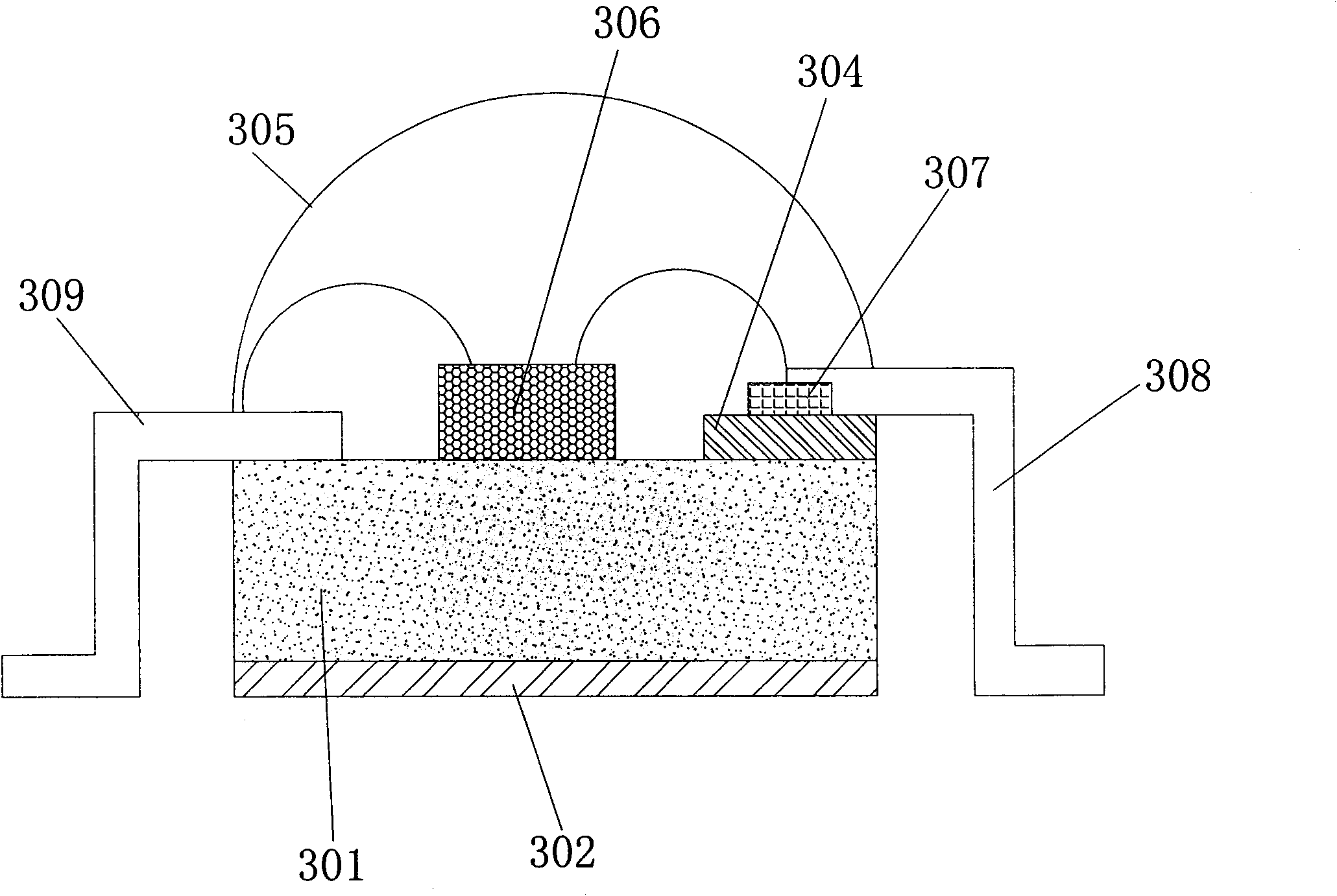
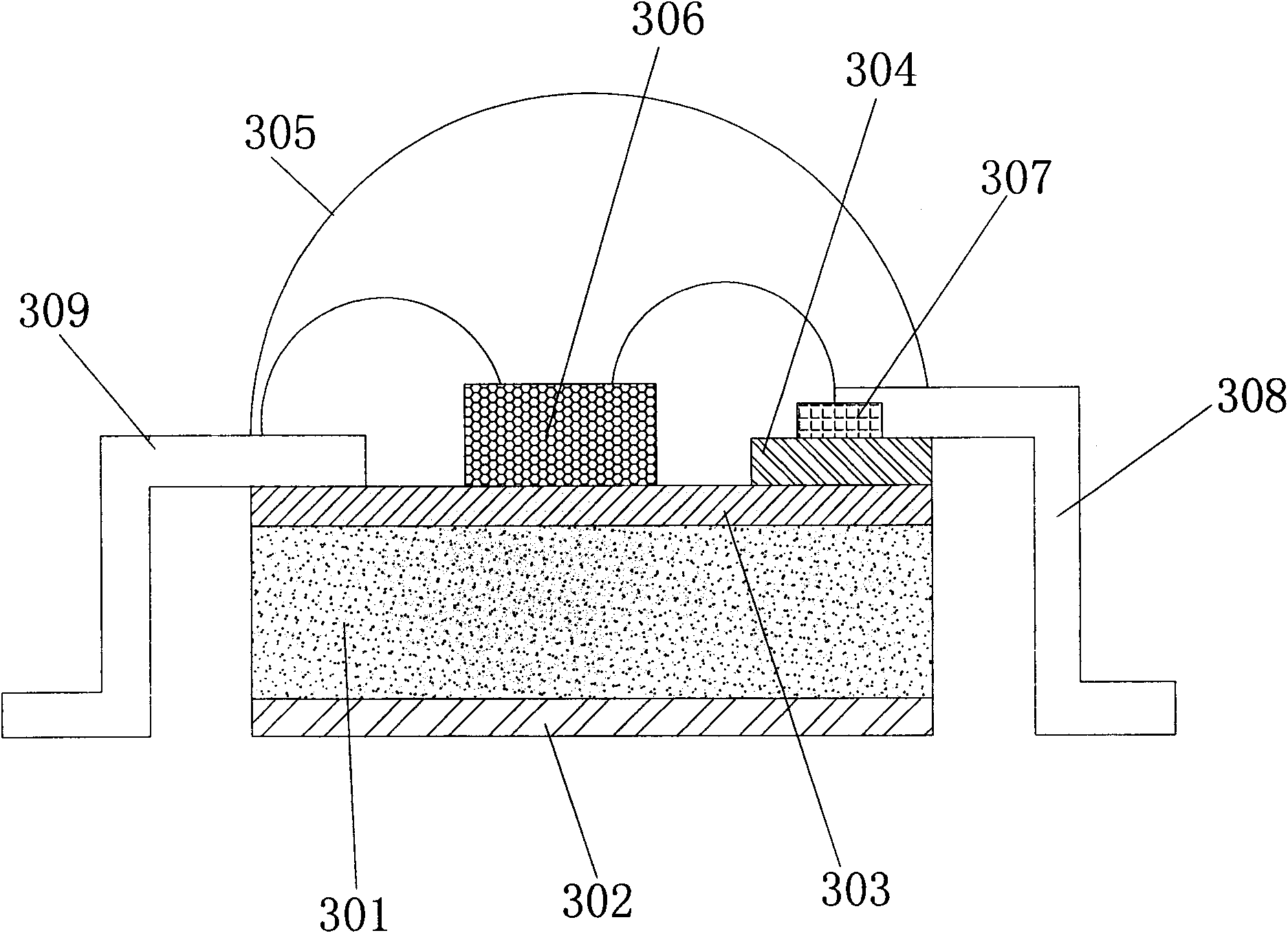
Embodiment 2
[0047] In Embodiment 2, the bottom of the metal substrate 301 is set as a rough bottom surface, and a layer of ceramic insulating layer (ie, the second insulating layer 302 ) is fabricated on the rough bottom surface of the bottom of the metal substrate by thermal spraying. In this embodiment, the first external electrode 308 and the second external electrode 309 are respectively welded on the metal electrode layer 307 and the metal heat conducting layer 303 by ultrasonic welding or resistance welding. The metal electrode layer 307 is melted and attached to the glass-ceramic insulating layer by means of laser ablation.
[0048] The laser ablation and melting method is used to form the required glass ceramic insulating layer and metal electrode layer, which avoids the overall high-temperature sintering, does not need to use a high-temperature sintering process, saves energy, is environmentally friendly, expands the types of optional metal substrate materials, and is easy to real...
PUM
 Abstract
Description
Claims
Application Information