Nonvolatile memory with error detection/correction circuit and reading and writing method thereof

An error correction circuit and memory technology, applied in static memory, memory system, read-only memory, etc., can solve the problems of reducing the service life of EEPROM, wasting writing operation space, and reducing storage flexibility, so as to save area cost and reduce usage Influence of lifespan, effect of improving flexibility

Active Publication Date: 2010-12-29
GIGADEVICE SEMICON (BEIJING) INC
View PDF0 Cites 9 Cited by
  • Summary
  • Abstract
  • Description
  • Claims
  • Application Information

AI Technical Summary

Problems solved by technology

However, in the process of realizing the present invention, the inventor found that when reading and writing inside the memory, what the prior art uses is the ECC code word of multi-byte data bits, especially when writing new data to the internal storage array, it is It is operated with a larger space unit such as a page (Page, 128KB). If the amount of input data is less than one page (this situation is very common at present), it will increase the writing time and greatly reduce the storage flexibility. The space for write operation is wasted, and unnecessary erase / program operation during operation will greatly reduce the service life of EEPROM

Method used


Image

  • Nonvolatile memory with error detection/correction circuit and reading and writing method thereof
  • Nonvolatile memory with error detection/correction circuit and reading and writing method thereof
  • Nonvolatile memory with error detection/correction circuit and reading and writing method thereof

Examples


Embodiment Construction

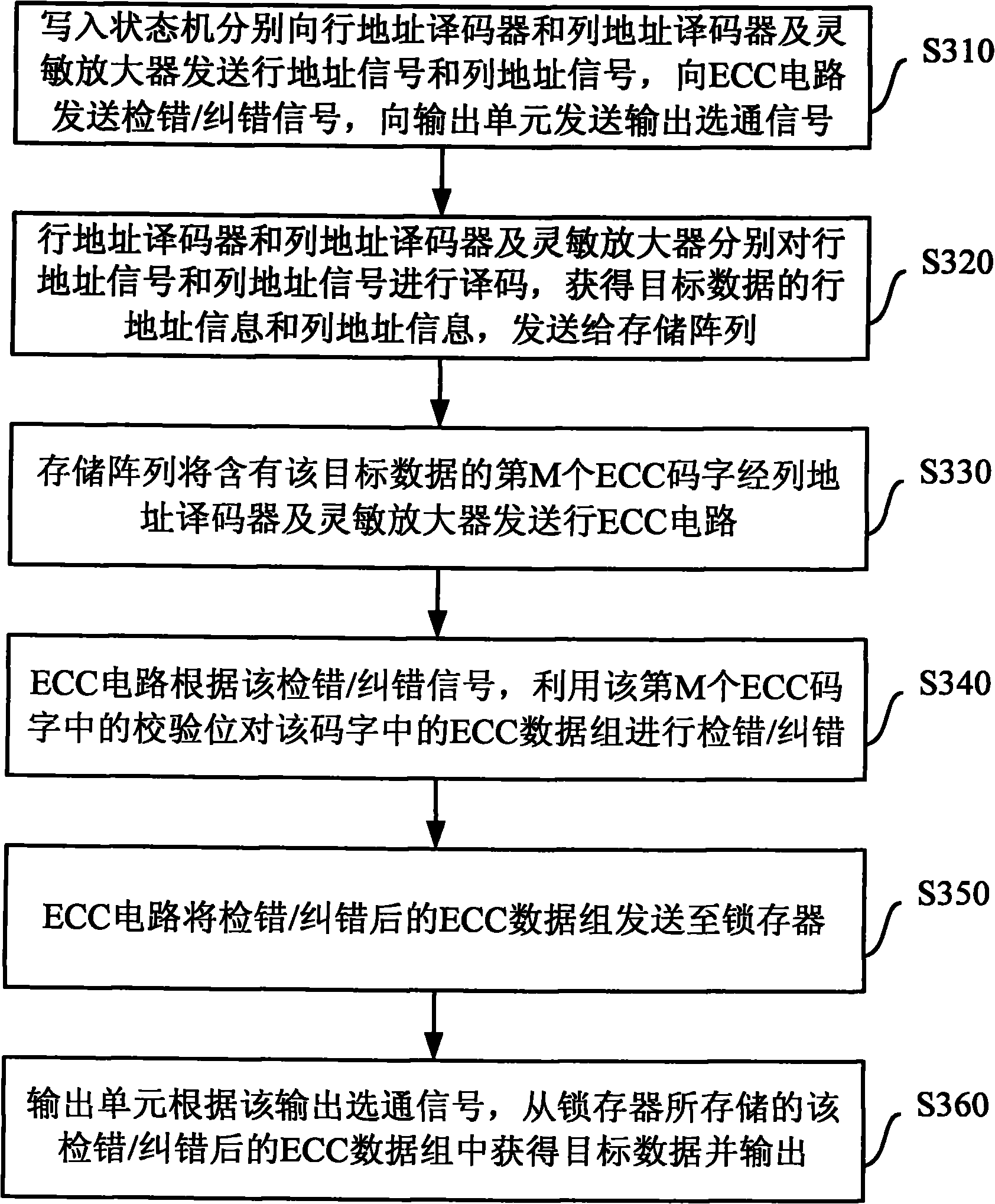
[0044] The implementation of the present invention will be described in detail below in conjunction with the accompanying drawings and examples, so as to fully understand and implement the process of how to apply technical means to solve technical problems and achieve technical effects in the present invention.

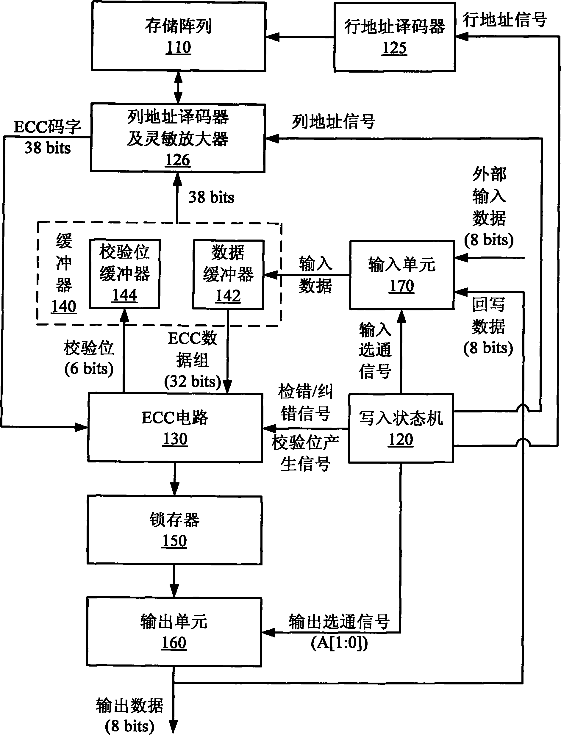
[0045] figure 1 It is a schematic composition diagram of an embodiment of the non-volatile memory of the present invention, and the external interface of the non-volatile memory transmits data in units of bytes. In this embodiment, the ECC code word is 38 bits, including an ECC data set (ECC data set) and check bits, wherein the ECC data set is 32 bits, and the check bits are 6 bits. With 8 bits as a byte (byte), the ECC data group has a total of 4 bytes (at least two bytes). Unless otherwise specified below, in the following embodiments of the present application, one ECC data group contains 4 bytes, and one byte contains 8 bits.

[0046] Such as figure 1As shown,...


PUM


Abstract

The invention discloses a nonvolatile memory with an ECC circuit and a reading and writing method thereof. An external interface of the memory performs data transmission by taking a byte as a unit; and the reading and writing is performed in the memory by taking an ECC code word as a unit. The method for writing data comprises the following steps of: acquiring a starting address and an end address of external input data and caching the external input data; if partial bytes of an ECC data set in which the external input data is positioned are not needed to be replaced, acquiring the bytes not needed to be replaced, namely write back data from a storage array of the nonvolatile memory and caching the write back data; forming a new ECC data set by the external input data, or the external input data and the write back data, and generating a corresponding check bit for the new ECC data set; and writing the new ECC data set and the corresponding check bit into the storage array. When the data is written, the corresponding ECC code word is only erased. The invention has the advantages of improving storage flexibility and the utilization rate of the storage space.

Description

technical field [0001] The invention relates to a non-volatile memory, in particular to a non-volatile memory with an error checking / correcting (Error Checking and Correcting, ECC) circuit and a reading and writing method thereof. Background technique [0002] With the rapid development of integrated circuits, the integration level of semiconductor memory is getting higher and higher, and the capacity is also getting larger. The ensuing problem is that the reliability and yield of semiconductor memory are facing serious challenges. For example, the signal-to-noise ratio decreases with the increase of integration, and the decrease of the charge of the storage node makes the storage unit more susceptible to the influence of cosmic rays. , The process deviation and material defects under the deep submicron technology lead to the reduction of the yield of the memory, etc. [0003] Error-correcting codes are a type of codes that can not only detect errors but also locate and cor...

Claims


Application Information

Patent Timeline
Patent Type & Authority Applications(China)
IPC IPC(8): G06F12/00G11C16/06G11C16/02G11C11/34
Inventor 苏如伟
Owner GIGADEVICE SEMICON (BEIJING) INC
Why Eureka
Try Eureka