Manufacturing method of packaging base plate provided with side surface lines

A manufacturing method and surface circuit layer technology, applied in semiconductor/solid-state device manufacturing, circuits, electrical components, etc., can solve problems such as difficulty, high manufacturing cost, and difficulty in improving yield

Active Publication Date: 2012-07-18
ASE SHANGHAI
View PDF0 Cites 0 Cited by
  • Summary
  • Abstract
  • Description
  • Claims
  • Application Information

AI Technical Summary

Problems solved by technology

However, the problem with this improved technology is that as the substrate unit becomes increasingly miniaturized, the diameter of the plated-through hole becomes smaller, and it is not easy to accurately cut the plated-through hole into two symmetrical half-plated through-holes. Therefore, the yield of the entire manufacturing process is difficult to improve, and will lead to high manufacturing costs

Method used


Image

  • Manufacturing method of packaging base plate provided with side surface lines
  • Manufacturing method of packaging base plate provided with side surface lines
  • Manufacturing method of packaging base plate provided with side surface lines

Examples


Embodiment Construction

[0026] In order to make the above objectives, features and advantages of the present invention more obvious and understandable, the following is a detailed description of the preferred embodiments of the present invention in conjunction with the accompanying drawings:

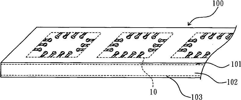
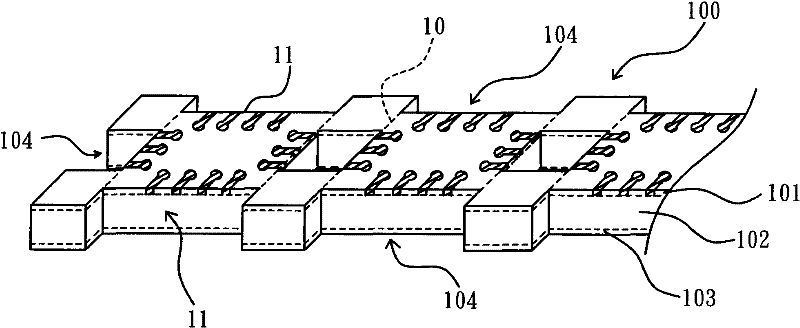
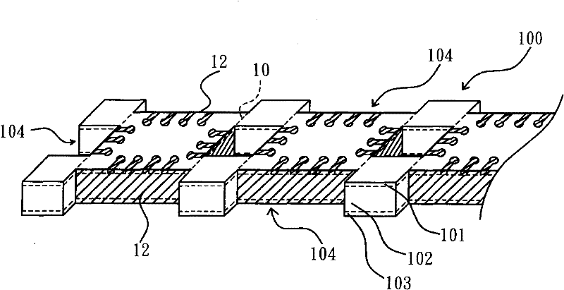
[0027] The method for manufacturing a package substrate with side surface circuits of the first embodiment of the present invention is mainly used to manufacture single-layer or multi-layer circuit substrates for semiconductor packaging, and can be further used to construct various package structures with substrates For example, ball grid array packaging (BGA), pin array packaging (PGA), contact array packaging (LGA), or chip-on-substrate packaging (BOC), etc., but not limited to these. The present invention will cooperate below Figure 1A to 1E The specific technical content of each step of the first embodiment is described in detail one by one.

[0028] Please refer to Figure 1A As shown, the first step of the met...


PUM


Abstract

The invention discloses a manufacturing method of a packaging base plate provided with side surface lines. The manufacturing method comprises the following steps of: providing a base plate bar which defines a plurality of base plate units; cutting a plurality of notches on a plurality of sides of the base plate unit of the base plate bar to expose the plurality of side surfaces of the base plate unit, two adjacent side surfaces of the base plate unit sharing the same notch; forming a conductive coating on each side surface of the base plate unit; processing the conductive coating to form a side surface line layer; and cutting the base plate bar to separate the at least one base plate unit after the side surface line layer is machined and formed.

Description

【Technical Field】 [0001] The present invention relates to a method for manufacturing a substrate for packaging with side surface circuits, and more particularly to a method for manufacturing a substrate for packaging that utilizes slotting of a substrate strip to form side surface circuits on the side surface of a substrate unit. 【Background technique】 [0002] Nowadays, the semiconductor packaging industry has gradually developed various types of packaging structures in order to meet the needs of various high-density packaging. Among them, common packaging structures with substrates include ball grid array (BGA), Pin grid array (PGA), land grid array (LGA), or board onchip (BOC), etc. In the above-mentioned packaging structure, an upper surface of the substrate carries at least one chip, and several pads of the chip are electrically connected to the substrate through a wire bonding or bumping manufacturing process. Several pads on the upper surface. At the same time, a large n...

Claims


Application Information

Patent Timeline
Patent Type & Authority Patents(China)
IPC IPC(8): H01L21/48H01L23/13H01L23/498
CPCH01L2924/0002
Inventor 任金虎高洪涛罗光淋方仁广林聪志孙骐
Owner ASE SHANGHAI
Why Eureka
Try Eureka