A/D converter circuit and solid-state imaging device

A technology for converting circuits and circuits, applied in the direction of analog/digital conversion, code conversion, analog-to-digital converter, etc.

Active Publication Date: 2011-01-05
思特威(上海)电子科技股份有限公司
View PDF5 Cites 12 Cited by
  • Summary
  • Abstract
  • Description
  • Claims
  • Application Information

AI Technical Summary

Problems solved by technology

[0033] In addition, in the case of the column-parallel A/D conversion circuit described in Patent Document 2, for example, when the number of digits of digital data is 10, the number of high-order digits is 5, and the...

Method used


Image

  • A/D converter circuit and solid-state imaging device
  • A/D converter circuit and solid-state imaging device
  • A/D converter circuit and solid-state imaging device

Examples


no. 1 approach

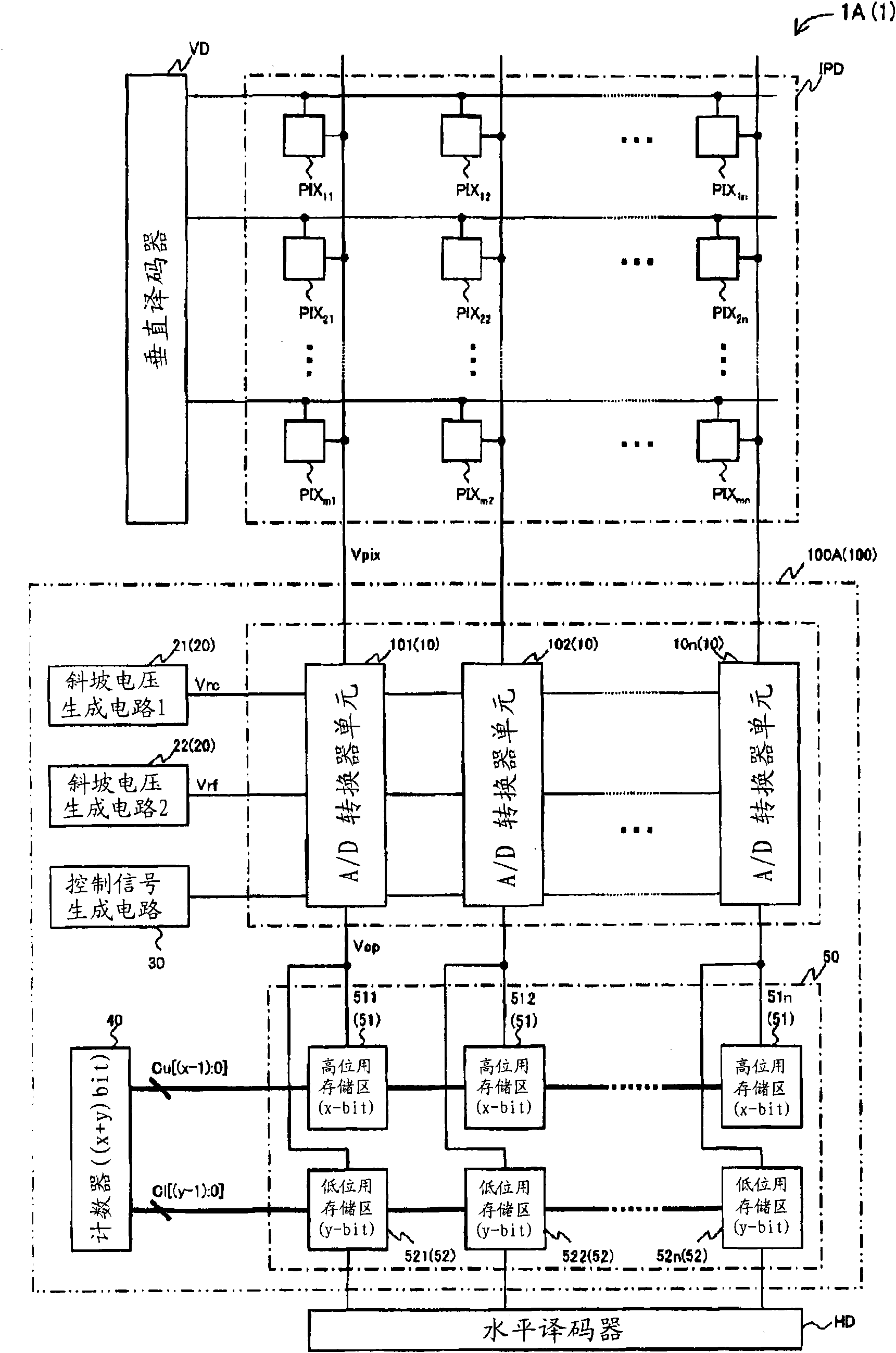
[0133] based on Figure 1 ~ Figure 3 A first embodiment of the circuit of the present invention and the device of the present invention will be described.

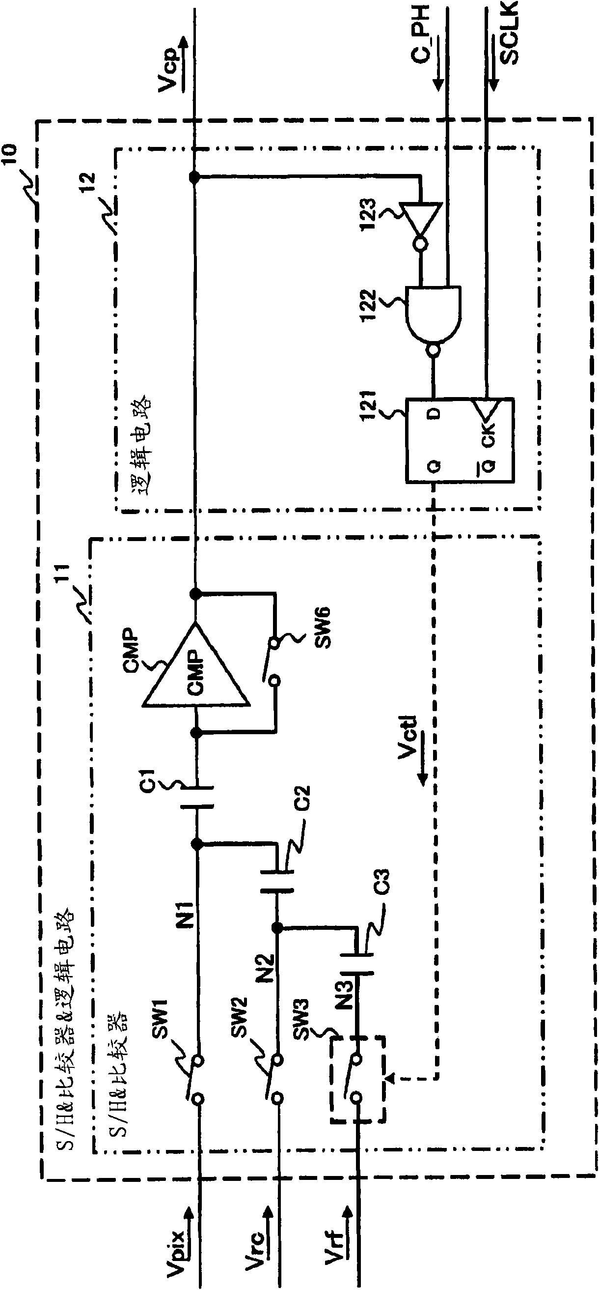
[0134] First, based on figure 1 and figure 2 The structure of the circuit of the present invention and the device of the present invention will be described. here, figure 1 A schematic configuration example of a device 1A of the present invention equipped with a circuit 100A of the present invention is shown, figure 2 A schematic configuration example of the circuit 100A of the present invention according to the present embodiment is shown.

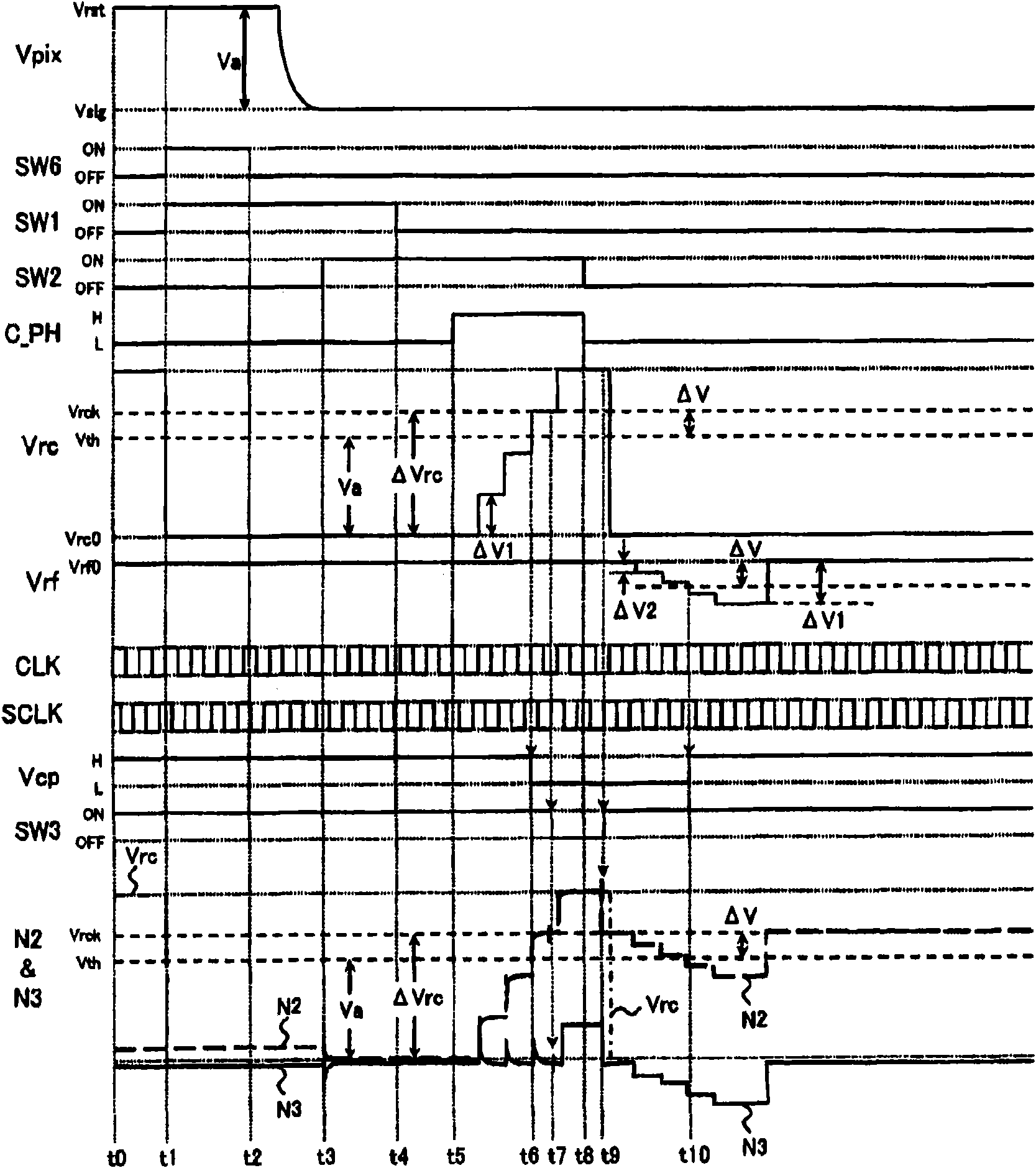
[0135] In addition, the circuit 100A of the present invention is a partitioned A / D conversion circuit that performs a two-stage conversion process of the first conversion process and the second conversion process. The value of a part of consecutive bits including the highest bit in the data; the above-mentioned second conversion process obtains the value of the unconverted bi...

no. 2 approach

[0196] based on Figure 4 ~ Figure 6 A second embodiment of the circuit of the present invention and the device of the present invention will be described. In addition, in this embodiment, the case where the configurations of the A / D conversion unit and the first ramp voltage generating circuit are different from those of the first embodiment described above will be described.

[0197] First, based on Figure 4 and Figure 5 The structure of the circuit of the present invention and the device of the present invention will be described. here, Figure 4 A schematic configuration example of an inventive device 1B equipped with an inventive circuit 100B according to the present embodiment is shown, Figure 5 A schematic configuration example of the circuit 100B of the present invention according to this embodiment is shown.

[0198] like Figure 4 As shown, similarly to the first embodiment, the device 1B of the present invention is configured to include, on the same chip, a...

no. 3 approach

[0237] based on Figure 7 (b) A third embodiment of the circuit of the present invention and the device of the present invention will be described. In addition, in this embodiment, the case where the structure of the 2nd ramp voltage Vrf differs from the said 1st Embodiment and 2nd Embodiment is demonstrated. here, Figure 7 (b) shows the structure of the second ramp voltage Vrf in this embodiment; Figure 7 (a) The second ramp voltage Vrf of the first and second embodiments described above is shown as a comparison object of the second ramp voltage Vrf of the present embodiment.

[0238] First, the structures of the circuit 100A of the present invention and the device 1 of the present invention will be briefly described based on the drawings. like figure 1 As shown, similarly to the first embodiment, the device 1 of the present invention is configured to include, on the same chip, a solid-state imaging device group IPD, and a plurality of A / D conversion units individually...


PUM


Abstract

Provided are a solid-state image pickup device and subranging A/D converter circuit that can effectively realize both preventing the conversion accuracy from degrading due to characteristic variations and preventing the circuit scale from increasing. There are included series-connected capacitive elements (C1-C3); a voltage comparator circuit (CMP) that compares an output value of the capacitive element (C1) with a threshold voltage value (Vth); a first input circuit that supplies an analog voltage signal (Vpix), which is to be converted, to a node between the capacitive elements (C1 and C2);a second input circuit that supplies a first reference voltage, the voltage value of which monotonously varies, to a node between the capacitive elements (C2 and C3) during execution of a first conversion process obtaining the values of higher-order bits; a third input circuit that supplies a second reference voltage, the voltage value of which monotonously varies, to an input terminal of the capacitive element (C3) during execution of a second conversion process obtaining the values of unconverted bits after completion of the first conversion process; and a control circuit (12) that generates a control signal (Vctl) for holding the first reference voltage in the capacitive element (C3) at occurrence of a change in the output of the voltage comparator circuit (CMP) in the first conversionprocess.

Description

technical field [0001] The present invention relates to an A / D conversion circuit for converting an analog signal into a digital signal, and particularly to a solid-state imaging device in which a plurality of solid-state imaging elements for converting an optical signal into an electrical signal are arranged in a matrix. A column-parallel A / D conversion circuit mounted on the same chip. Background technique [0002] A solid-state imaging element (unit pixel) that converts an optical signal into an electrical signal by photoelectric conversion, etc., including a plurality of CMOS imaging sensors, CCD sensors, near-infrared imaging sensors, and far-infrared imaging sensors, etc. is arranged as Among the solid-state imaging devices of the solid-state imaging device group formed in a matrix, there are devices in which analog circuits, digital circuits, and the like are mounted on the same chip. [0003] As a circuit mounted on the same chip as the solid-state imaging element g...

Claims


Application Information

Patent Timeline
IPC IPC(8): H03M1/14H03M1/56H04N5/335H04N5/365H04N5/374H04N5/378
CPCH03M1/56H03M1/123H03M1/144H04N5/3742H04N5/378H04N25/767H04N25/75
Inventor 星野幸三
Owner 思特威(上海)电子科技股份有限公司
Why Eureka
Try Eureka