Grain bearing part structure of lead frame for semiconductor capsulation

A lead frame and carrier technology, applied in the lead frame field, can solve the problems of increased junction resistance, influence on welding quality, open circuit, etc., and achieve the effect of improving bonding strength

Inactive Publication Date: 2011-01-12
GTM
View PDF0 Cites 3 Cited by
  • Summary
  • Abstract
  • Description
  • Claims
  • Application Information

AI Technical Summary

Problems solved by technology

[0006] Generally, silver glue, non-conductive glue or solder is used to weld the die 10 on the die carrier 20, so it is possible that the silver glue, non-conductive glue or solder will pollute the area near the die 10 during soldering, especially It is the wire pad 24 of the die carrier 20, which affects the welding quality between the wire pad 24 and the wire 40, resulting in poor welding, increased junction resistance, or even an open circuit due to empty soldering
[0007] In addition, because the die carrier 20 can be directly attached to the circuit board, the thermal stress and mechanical stress on the bonding wire pad 24 of the die carrier 20 will increase, that is, due to the thermal expansion coefficient of the packaging material and the soldering The wire pad 24 is different, so in the process of heating up or cooling and shrinking, thermal stress and mechanical stress will be formed on the welding wire 40 welded on the wire pad 24, resulting in the welding wire on the wire pad 24 40 stripped

Method used


Image

  • Grain bearing part structure of lead frame for semiconductor capsulation
  • Grain bearing part structure of lead frame for semiconductor capsulation
  • Grain bearing part structure of lead frame for semiconductor capsulation

Examples


Embodiment Construction

[0035] The embodiments of the present invention will be described in more detail below in conjunction with the drawings and component symbols, so that those skilled in the art can implement them after studying this specification.

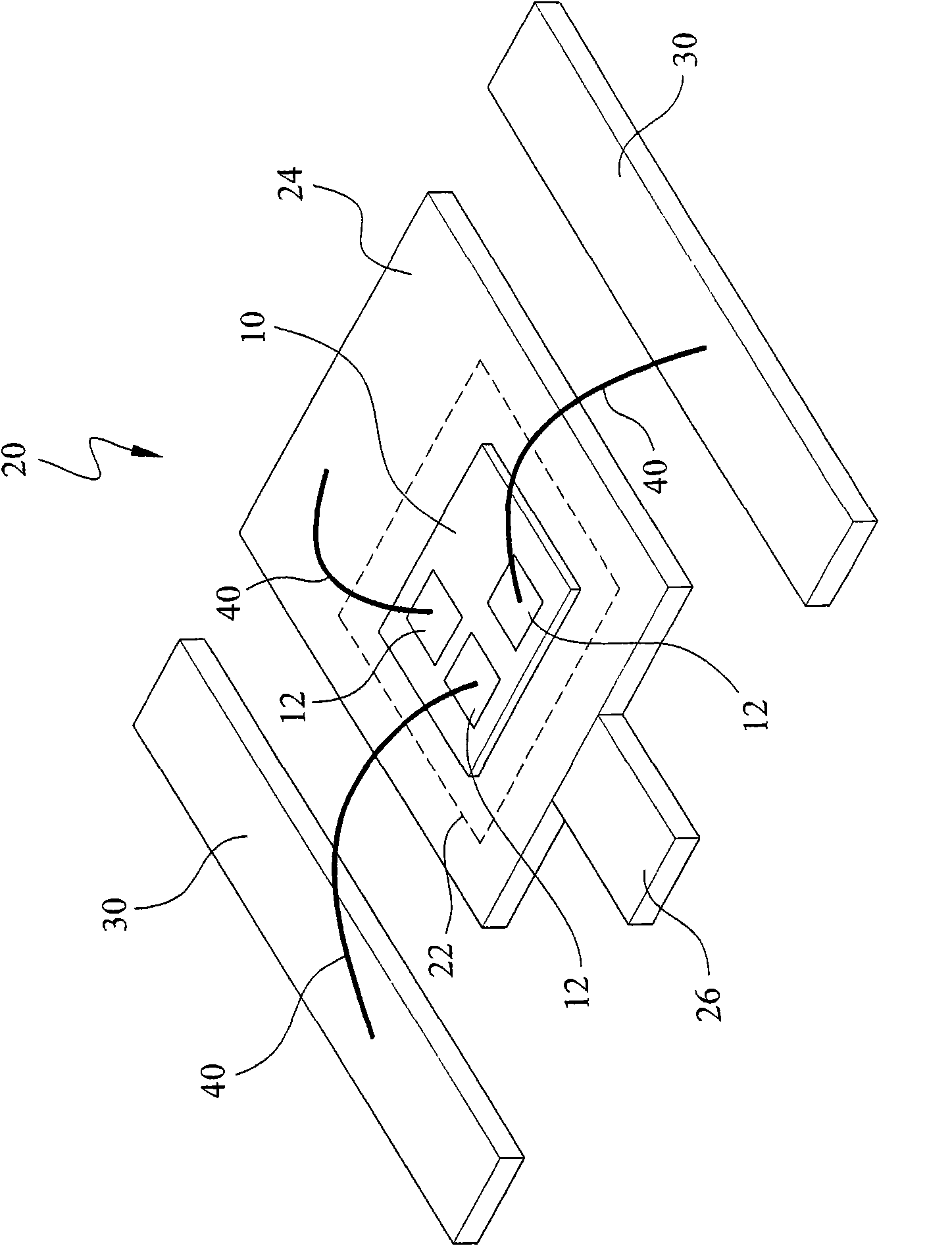
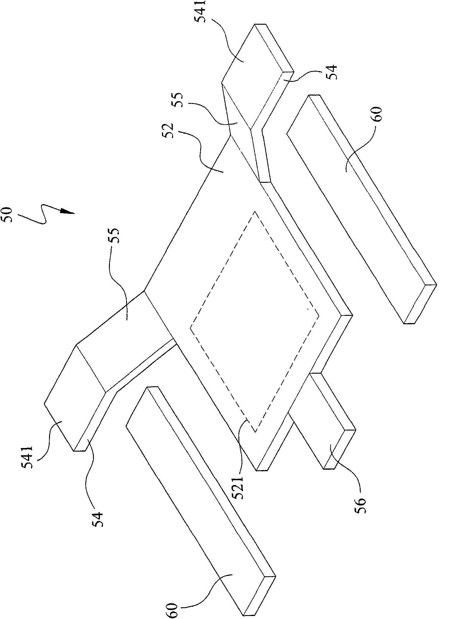
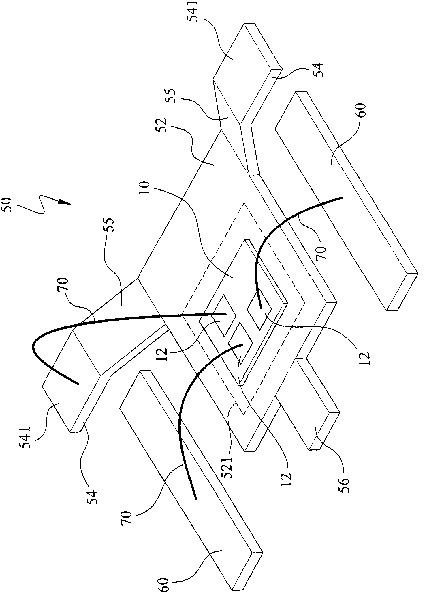
[0036] refer to figure 2 , a schematic diagram of the lead frame of the present invention. The lead frame includes a die carrier 50 and a plurality of leads 60 . Wherein the die carrier 50 is not connected to the leads 60 , the die carrier 50 has a die region 52 , at least one bonding wire region 54 , and at least one connection portion 55 . It should be noted that, for the convenience of describing the features of the present invention, the present embodiment uses the two wire bonding regions 54 and the two connecting portions 55 as exemplary examples for illustration, so the number of the bonding wire regions 54 and the connecting portions 55 is essentially Can contain any positive integer. In addition, in this embodiment, there is also a pin ...


PUM


Abstract

The invention discloses a grain bearing part structure of a lead frame for semiconductor capsulation. A grain bearing part mainly comprises a grain zone, at least one bonding wire zone and at least one connecting part, wherein a grain bonding pad is arranged on the surface of the grain zone; a bonding wire pad is arranged on the surface of the bonding wire zone; and the bonding wire zone is connected with the grain zone through the connecting part. The invention can ensure that the position of the bonding wire pad is designed to be higher than that of the grain bonding pad; the grain bonding pad and the bonding wire pad are not on the same surface; and in addition, the bonding wire zone is not considered as a lead foot of the lead frame.

Description

technical field [0001] The invention relates to a lead frame for semiconductor packaging, in particular to a design in which the die pad and the wire pad included in the die carrier are not on the same plane. Background technique [0002] Generally, an integrated circuit (IC) includes a chip with electrical operation functions, a die carrier placed on a lead frame, and the lead frame also includes a plurality of bonding wire areas, gold wires are bonded to the chip's connection pads and bonding wires using a wire bonding process. The area connects the external pins through the bonding wire area, so that the connection pad of the chip is electrically connected with the corresponding external pins to transmit or receive electrical signals, and then the chip and the lead frame are covered with an insulating packaging material to provide electrical insulation and Protective effects. [0003] refer to figure 1 , a schematic diagram of a prior art leadframe. Such as figure 1 A...

Claims


Application Information

Patent Timeline
Patent Type & Authority Applications(China)
IPC IPC(8): H01L23/495H01L23/488H01L23/13
CPCH01L2224/48091H01L2224/48247
Inventor 张定宏
Owner GTM
Why Eureka
Try Eureka