SOI (Silicon on Insulator) CMOS (Complementary Metal Oxide Semiconductor) RF (Radio Frequency) switch and RF transmitter front-end module comprising same

A technology of radio frequency switch and switching tube, applied in the field of radio frequency, can solve problems such as complex structure and limited VH maximum value, and achieve the effect of simplifying structure and improving reliability

Inactive Publication Date: 2011-01-26
RDA MICROELECTRONICS BEIJING
View PDF4 Cites 22 Cited by
  • Summary
  • Abstract
  • Description
  • Claims
  • Application Information

AI Technical Summary

Problems solved by technology

[0006] In order to overcome the high level V in the prior art, the present invention H For the defects of limited maximum value and complex structure, provide SOI CMOS RF switch and RF transmit front-end module containing the RF switch

Method used


Image

  • SOI (Silicon on Insulator) CMOS (Complementary Metal Oxide Semiconductor) RF (Radio Frequency) switch and RF transmitter front-end module comprising same
  • SOI (Silicon on Insulator) CMOS (Complementary Metal Oxide Semiconductor) RF (Radio Frequency) switch and RF transmitter front-end module comprising same
  • SOI (Silicon on Insulator) CMOS (Complementary Metal Oxide Semiconductor) RF (Radio Frequency) switch and RF transmitter front-end module comprising same

Examples


Embodiment 1

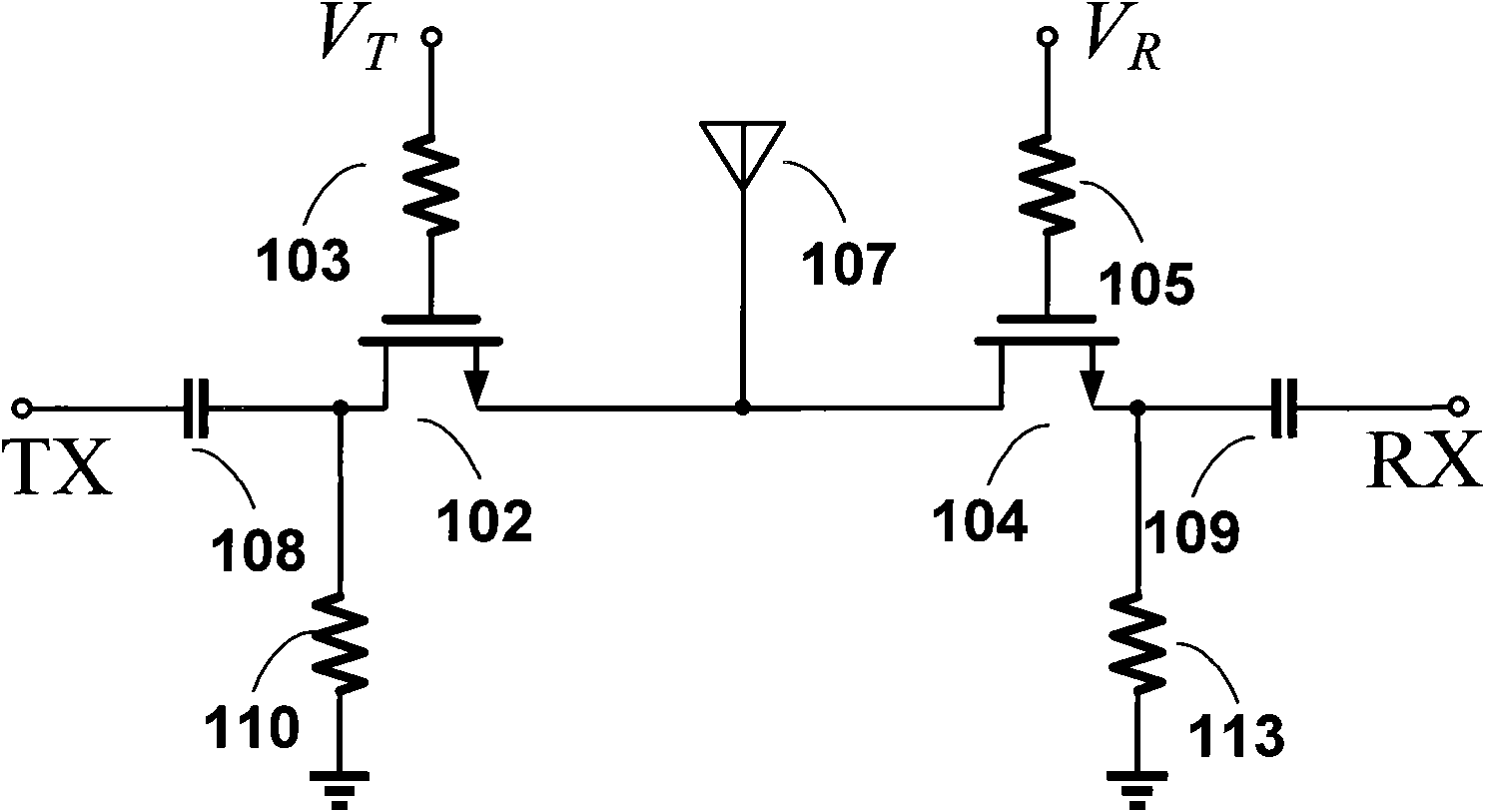
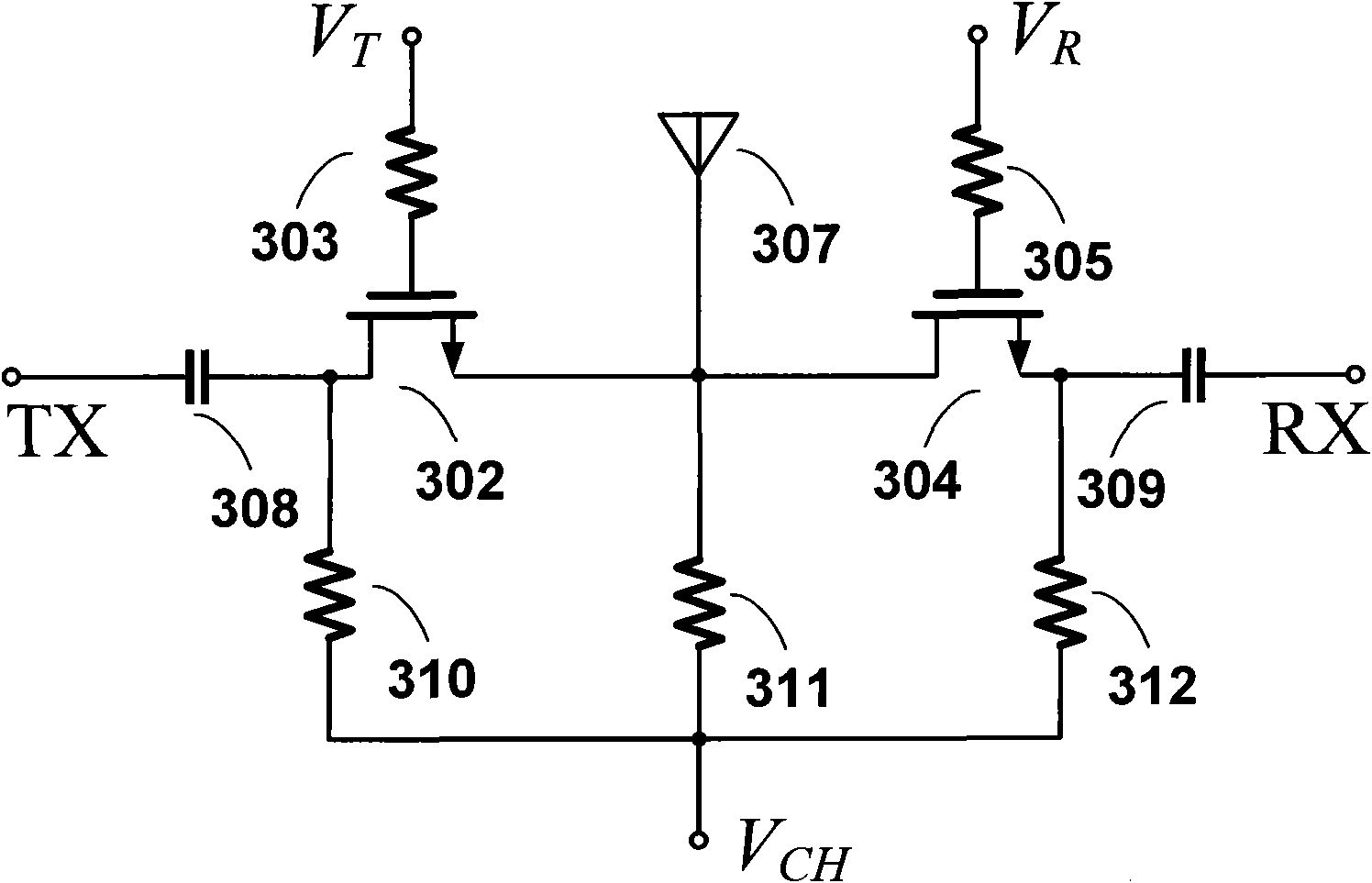
[0033] The structure of the first RF switch proposed by the present invention is as follows: image 3 shown. The transmit signal TX is connected to the drain of the transmit path switch tube 302 (NMOS tube) through the DC blocking capacitor 308; the source of the transmit path switch tube 302 is connected to the antenna 307, and is connected to the drain of the receive path switch tube 304 (NMOS tube) pole; the source of the receiving channel switch tube 304 is connected to the receiving signal RX through the DC blocking capacitor 309 . The gate of the emission path switch tube 302 is connected to the emission path control signal V through a resistor 303 T ; The gate of the receiving path switching tube 304 is connected to the receiving path control signal V through a resistor 305 R . In addition, one end of the resistor 310 is connected to the drain of the emission channel switch tube 302, and the other end is connected to the channel control voltage V CH ; One end of the...

Embodiment 3

[0040] The structure of the third RF switch proposed by the present invention is as follows: Figure 8 As shown, the switch is a single-pole three-throw switch, which can be used to select different radio frequency transmission signals TX1 , TX2 , TX3 to transmit to the antenna 807 . The transmission signal TX1 is connected to the drain of the transmission path switch tube 802 (NMOS tube) through the DC blocking capacitor 808; the source of the transmission path switch tube 802 is connected to the antenna 807, and connected to the drain of the transmission path switch tube 804 (NMOS tube) The pole is also connected to the drain of the transmission path switch tube 813 (NMOS tube); the source of the transmission path switch tube 804 is connected to the transmission signal TX3 through a DC blocking capacitor 809; the source of the transmission path switch tube 813 is passed through a DC blocking capacitor 814 Connect to transmit signal TX2. The gate of the emission path switch ...

Embodiment 4

[0044] The structure of the fourth RF switch proposed by the present invention is as follows: Figure 9 As shown, the switch is a single-pole three-throw switch, which can be used to select different transmit signals TX1 , TX2 , TX3 to transmit to the antenna 807 . The transmission signal TX1 is connected to the drain of the transmission path switch tube 802 (NMOS tube) through the DC blocking capacitor 808; the source of the transmission path switch tube 802 is connected to the antenna 807, and connected to the drain of the transmission path switch tube 804 (NMOS tube) The pole is also connected to the drain of the transmission path switch tube 813 (NMOS tube); the source of the transmission path switch tube 804 is connected to the transmission signal TX3 through a DC blocking capacitor 809; the source of the transmission path switch tube 813 is passed through a DC blocking capacitor 814 Connect to transmit signal TX2. The gate of the emission path switch tube 802 is connect...


PUM


Abstract

The invention relates to an SOI (Silicon On Insulator) CMOS (Complementary Metal Oxide Semiconductor) RF (Radio Frequency) switch and an RF transmitter front-end module comprising the same. The SOI CMOS RF switch comprises a plurality of DC-blocking capacitors, a plurality of resistors and a plurality of switching tubes, wherein the switching tubes are SOI CMOS switching tubes, the drain electrode of each switching tube is connected to a channel control voltage through a resistor, the source electrode of each switching tube is connected to the channel control voltage through another resistor and connected with an antenna, and the channel control voltage is larger than 0 V and smaller than the difference of a high level and a threshold voltage of the switching tube. At the same moment, only one switching tube has a control signal at a high-level voltage, and the other switching tubes have control signals at the voltage of 0 V. The technical scheme provided by the invention simplifies the structure of the RF switch; and the RF switch can work under a signal power supply to ensure that the control signal voltage in a switching transistor in each SOI CMOS RF switch can be higher than the safe voltage of the transistor, thus the reliability of the RF switch is improved.

Description

technical field [0001] The invention relates to the radio frequency field, in particular to an SOI CMOS radio frequency switch and a radio frequency transmitting front-end module including the radio frequency switch. Background technique [0002] With the continuous development of modern wireless communication technology, there has been a situation where multiple communication standards coexist, such as GSM, WCDMA, CDMA, TD-SCDMA and so on. In order to make the same wireless communication mobile phone terminal available all over the world, it is required that the mobile phone terminal must support these different communication standards at the same time. Therefore, multiple radio frequency power amplifiers supporting different communication standards are required in the mobile terminal, and a radio frequency switch is used to switch the required radio frequency power amplifiers to the transmission channel. At the same time, radio frequency switches can also be used to switc...

Claims


Application Information

Patent Timeline
Patent Type & Authority Applications(China)
IPC IPC(8): H03K17/74H04B1/02
CPCH04B1/48
Inventor 袁志鹏王宇晨
Owner RDA MICROELECTRONICS BEIJING
Why Eureka
Try Eureka