Slow light waveguide structure based on photonic crystal air bridge structure

A technology of photonic crystal and waveguide structure, which is applied in the direction of light guide, optics, optical components, etc., can solve the problems that the design of large bandwidth has not been reported yet, the design is more difficult, and it is difficult to meet the large bandwidth of optical communication.

Inactive Publication Date: 2012-09-26
INST OF SEMICONDUCTORS - CHINESE ACAD OF SCI
View PDF0 Cites 0 Cited by
  • Summary
  • Abstract
  • Description
  • Claims
  • Application Information

AI Technical Summary

Problems solved by technology

[0004] The photonic crystal slow-light effect waveguide is the basis for the design of photonic crystal slow-light devices. Previously, many literatures reported that photonic crystal line defects can be used as slow-light devices, and the group refractive index can reach more than 100, but the design of large bandwidth has not been reported. Here We define the slow light operating bandwidth as the single-mode continuous operating region with a group refractive index greater than 10
Ordinary slow-light photonic crystal waveguide bandwidth is several nanometers, so it is difficult to meet the requirements of large bandwidth in optical communication
In addition, the working wavelength position is generally changed by adjusting the lattice period of the photonic crystal by keeping the duty cycle constant. In this way, the devices required for different working areas require different process conditions, which makes the design more difficult.

Method used


Image

  • Slow light waveguide structure based on photonic crystal air bridge structure
  • Slow light waveguide structure based on photonic crystal air bridge structure
  • Slow light waveguide structure based on photonic crystal air bridge structure

Examples


Embodiment Construction

[0028] In order to make the object, technical solution and advantages of the present invention clearer, the present invention will be described in further detail below in conjunction with specific embodiments and with reference to the accompanying drawings.

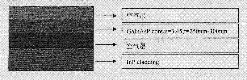
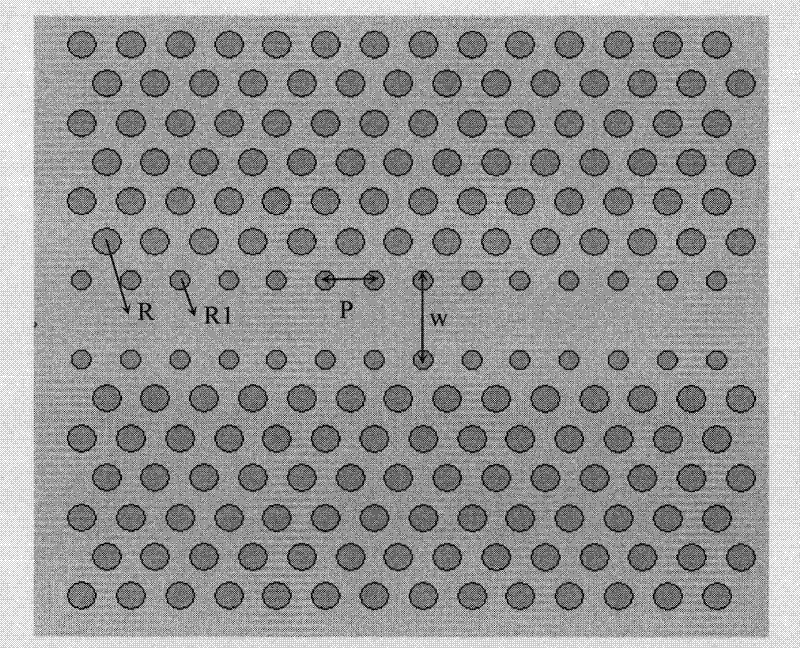
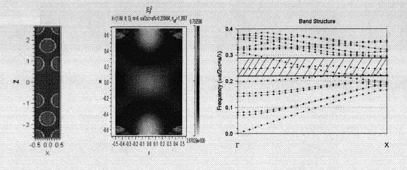
[0029] The existing photonic crystal slow light waveguide, the slow light working area (the area where the group refractive index is greater than 10 is defined here) is relatively small, generally a few nanometers, and the adjustment of the central working wavelength needs to be realized by maintaining the duty ratio and adjusting the lattice period. This requires high design and process requirements. Different operating wavelengths require different process conditions to achieve, or complex design parameter adjustments to match certain process conditions.

[0030] The present invention proposes a slow light waveguide structure based on a photonic crystal air bridge structure, which is a novel large bandwidth slow light ph...


PUM

PropertyMeasurementUnit
thicknessaaaaaaaaaa
refractive indexaaaaaaaaaa

Abstract

The invention discloses a slow light waveguide structure based on a photonic crystal air bridge structure, which adopts a line defect photonic crystal structure, and comprises a longitudinal structure and a horizontal structure, wherein, the longitudinal structure is an air bridge multi-layer structure which comprises an air layer, a semiconductor material layer, an air layer and a substrate material layer from the top layer to the bottom layer; the horizontal structure adopts a triangular lattice structure, the period is P, and the radius is R; and the waveguide is formed through removing a row of holes. Through changing the size of the line defect nearby hole, the slow light waveguide structure of the invention realizes a slow light working area reaching up to 50 nanometers; the centralwavelength can be adjusted through the width of the waveguide, which can be realized only in need of the small holes with two types of apertures within the requirement range of hundreds of nanometersof operating wavelengths, thus lowering the requirement of device parameter adjustment in a certain technological condition. By utilizing the slow light photonic crystal waveguide of the slow opticalwaveguide structure based on the photonic crystal air bridge structure, the bandwidth can cover the C wave band of the fiber-optical communication, and can achieve 50nm.

Description

technical field [0001] The invention relates to the technical field of photonic crystal slow light waveguide design and photonic optoelectronic device design, in particular to a slow light waveguide structure based on a photonic crystal air bridge structure. Background technique [0002] The slow light effect device is one of the key devices in the new generation of optical communication, optical storage and photonic devices. Due to its own characteristics, photonic crystals have been a research hotspot in recent years, and various effects have been discovered and utilized continuously. Almost all active and passive photonic devices can be designed and manufactured using the theory and materials of photonic crystals. Many of its unique features are eye-catching, such as the small-sized large-angle bending lossless waveguide based on the photonic crystal band gap, the superprism based on the large dispersion effect at the band edge, and the imaging lens that breaks through t...

Claims


Application Information

Patent Timeline
Patent Type & Authority Patents(China)
IPC IPC(8): G02F1/365G02F1/355G02B6/122
Inventor 张冶金郑婉华渠红伟陈良惠
Owner INST OF SEMICONDUCTORS - CHINESE ACAD OF SCI
Why Eureka
Try Eureka