CMOS (Complementary Metal-Oxide-Semiconductor) inverter pair based method and circuit for designing high-speed chaotic oscillator

A design method, inverter technology, applied in power oscillators, electrical components, digital transmission systems, etc.

Inactive Publication Date: 2011-02-02
ZHEJIANG UNIV
View PDF3 Cites 0 Cited by
  • Summary
  • Abstract
  • Description
  • Claims
  • Application Information

AI Technical Summary

Problems solved by technology

The negative resistance sub-circuits in traditional Chua's circuits are mostly constructed based on operational amplifiers. The speed of operational amplifiers limits the oscillation frequency of Chua's circuits, making the fundamental frequency of chaotic signals generated by traditional Chua's circuits mostly in the kHz order

Method used


Image

  • CMOS (Complementary Metal-Oxide-Semiconductor) inverter pair based method and circuit for designing high-speed chaotic oscillator
  • CMOS (Complementary Metal-Oxide-Semiconductor) inverter pair based method and circuit for designing high-speed chaotic oscillator
  • CMOS (Complementary Metal-Oxide-Semiconductor) inverter pair based method and circuit for designing high-speed chaotic oscillator

Examples


Embodiment Construction

[0023] The present invention will be further described below in conjunction with drawings and embodiments.

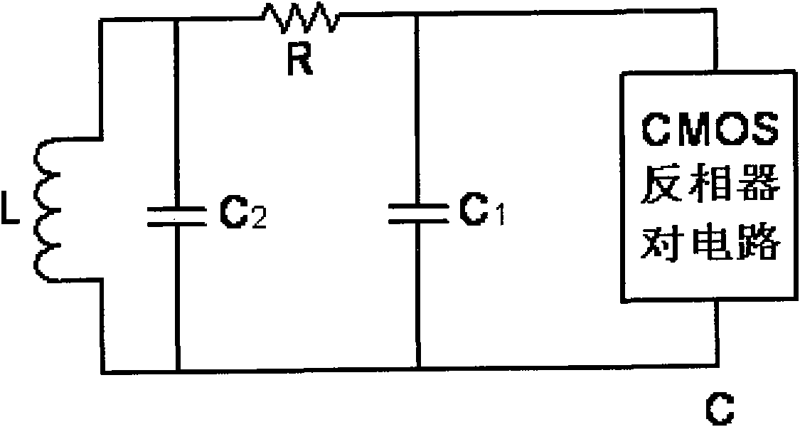
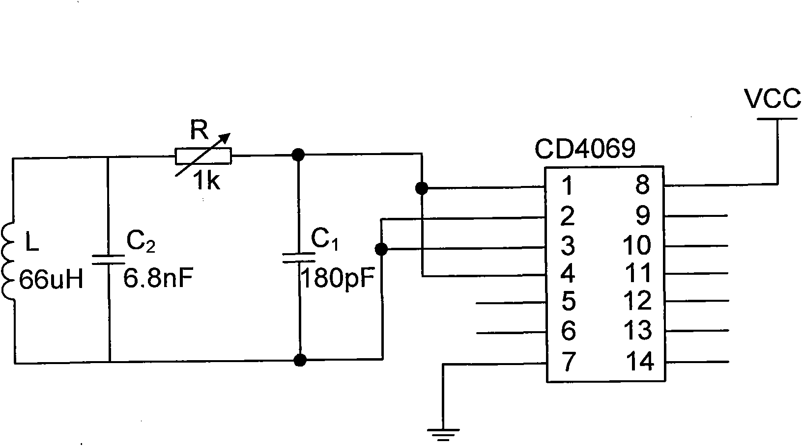
[0024] Such as figure 1 As shown, the chaotic oscillator of the present invention is based on the traditional Chua's circuit, and the negative resistance circuit formed by the CMOS inverter pair circuit is used to replace the negative resistance circuit based on the operational amplifier in the traditional Chua's circuit to generate faster chaotic oscillation .

[0025] Such as figure 1 Shown, the circuit structure of the present invention is: one end of inductance L and electric capacity C 2 One end of the resistor R is connected to one end of the resistor R, the other end of the resistor R and the capacitor C 1 One end of the CMOS inverter is connected to one end of the circuit, the other end of the inductor L, the capacitor C 2 the other end of the capacitor C 1 The other end of is connected with the other end of the CMOS inverter pair circuit.

[0026] On the ...


PUM


Abstract

The invention discloses a CMOS (Complementary Metal-Oxide-Semiconductor) inverter pair based method and a circuit for designing a high-speed chaotic oscillator. In the invention, a negative resistance circuit consisting of a CMOS inverter pair is used for replacing a negative resistance circuit based on an operational amplifier in a Chua's circuit to generate chaotic oscillation; a CMOS inverter circuit consists of a chip CD4069 or consists of two PMOS (P-channel Metal Oxide Semiconductor) tubes and two NMOS (N-channel metal oxide semiconductor) tubes, inherits the characteristics of the traditional Chua's circuit and is used for generating chaotic oscillation signals; and when a CMOS inverter pair is used, i.e. two reversely connected inverters are used as a negative resistance circuit of an oscillator, the defect of lower working frequency of the traditional Chua's circuit can be overcome, and the inverter pair can work with a higher frequency, so that high-speed chaotic oscillation can be generated, and the working frequency reaches /MHz. The circuit can be designed and realized by using discrete devices, and the chip of the high-speed chaotic oscillator can be designed and realized by using a standard CMOS process, thus the circuit is beneficial to the manufacture and the production of chaotic signal sources in a large scale with low cost.

Description

technical field [0001] The invention relates to a design method and circuit of a high-speed chaotic oscillator, in particular to a design method and circuit of a high-speed chaotic oscillator based on a pair of CMOS inverters. Background technique [0002] The application of chaos in communication systems is a great impetus for the study of chaotic circuits. With the spread spectrum communication becoming more and more widely used, the application potential of chaotic spread spectrum communication in commercial wireless communication has attracted much attention. At present, a hot research direction of chaotic spread spectrum communication is to use the spread spectrum characteristics of chaotic signal itself, and use chaotic signal as carrier to carry out some innovative systems of chaotic carrier spread spectrum communication. In these researches, the design and implementation of high-speed chaotic oscillators are crucial. [0003] Chua's circuit is one of the most class...

Claims


Application Information

Patent Timeline
Patent Type & Authority Applications(China)
IPC IPC(8): H03B5/18H04L9/00
Inventor 史治国金梦珺陈积明洪少华
Owner ZHEJIANG UNIV
Why Eureka
Try Eureka