Organic electroluminescent device
An electroluminescent element and electroluminescent technology, which are applied to electroluminescent light sources, electrical components, organic semiconductor devices, etc., can solve the problems of small contact area and insufficient heat transfer effect, and achieve improved thermal radiation and simple structure. , Excellent heat dissipation effect
- Summary
- Abstract
- Description
- Claims
- Application Information
AI Technical Summary
Problems solved by technology
Method used
Image
Examples
Embodiment
[0201] Hereinafter, the present invention will be described in more detail while showing verification experiments and examples, but the present invention is not limited to the following examples and the like.
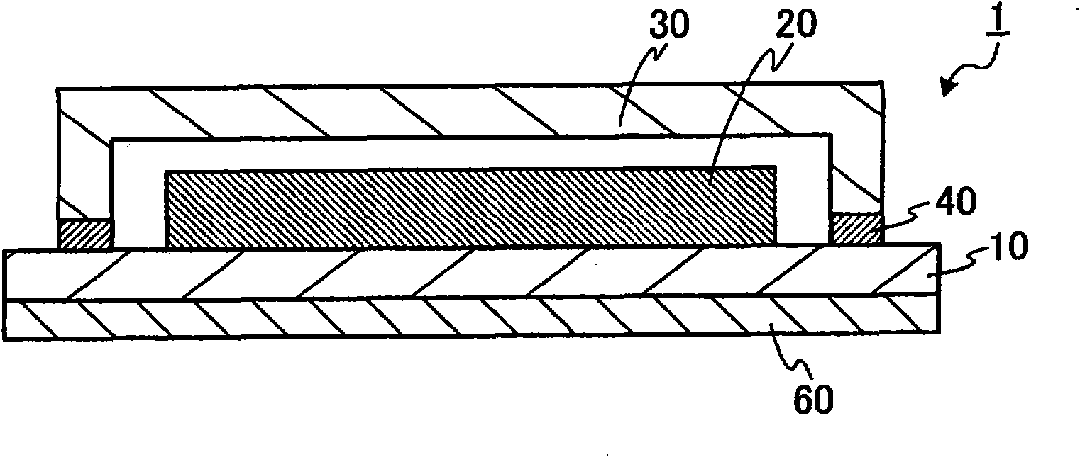
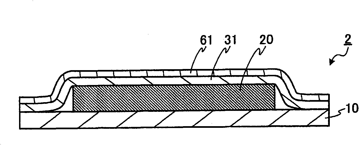
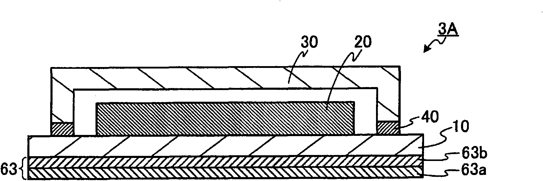
[0202] Validation experiments were performed using the Figure 5 The test setup shown was carried out. Considering that the present invention does not substantially depend on the structure of the laminated body of the organic EL element, a self-made point heater (point heater) is used as a heat source, and glass, an aluminum sheet covering a raw material with a high heat emissivity, etc. are used to evaluate. Such as Figure 5 As shown, a heating plate 81 is provided on a test stand 80, and a cylindrical heat conducting part 83 is provided at the center thereof. The heat conduction part 83 is made of brass, and the heat insulation sheet 82 is wound around the outer peripheral part of the side surface of the heat conduction part 83 . The test substrate holding glass ...
Embodiment 1
[0225] Fabrication of Bottom Emission Type Organic EL Elements
[0226] Bottom emission type organic EL elements were produced by the following method. First, a 200 mm x 200 mm glass substrate on which a plurality of ITO transparent conductive film patterns and Cr patterns for organic EL elements having a size of 30 mm x 40 mm were formed was produced. The ITO transparent conductive film was formed with a film thickness of about 150 nm by the sputtering method, and Cr was formed into a pattern of 200 nm by the sputtering method.
[0227] Next, on a glass substrate with ITO and Cr patterns, a suspension of poly(3,4)ethylenedioxythiophene / polystyrenesulfonic acid (manufactured by HC Stark, Baytron PTP AI 4083) was used to spin A film was formed by coating method, and dried in an oven at 200° C. for 20 minutes to form a hole injection layer with a thickness of 60 nm. Thereafter, the excess hole injection layer around the organic EL element was wiped with a water-soaked wiper t...
Embodiment 2
[0231] Fabrication of Bottom Emission Type Organic EL Elements
[0232] In Example 2, the material combination of the element substrate and the sealing substrate in the above-mentioned Example 1 is reversed. That is, the support substrate is a substrate coated with a high thermal conductivity material coated with black, and the sealing substrate is a glass substrate, which is fully sealed. As a result, for a so-called top emission type element that emits light from the sealing substrate side, an element having a uniform surface temperature distribution as in Example 1 can be produced.
PUM
 Abstract
Description
Claims
Application Information


