Method for forming asymmetrical transistor
A transistor and asymmetric technology, applied in semiconductor/solid-state device manufacturing, electrical components, circuits, etc., can solve problems such as increasing cost investment, achieve the effect of reducing capital investment and improving process window
- Summary
- Abstract
- Description
- Claims
- Application Information
AI Technical Summary
Problems solved by technology
Method used
Image

Examples
Embodiment Construction
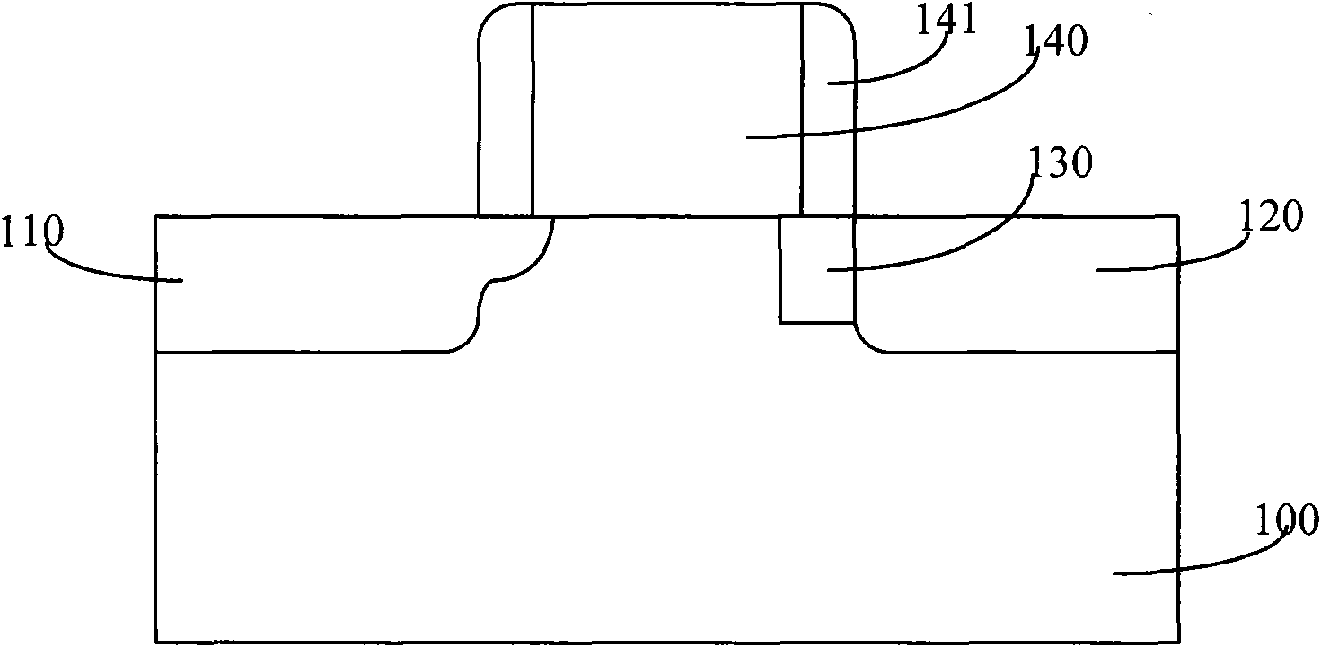
[0016] The inventors of the present invention have found that the existing process for forming pocket regions in transistors of asymmetric memory cells includes forming a separate photoresist pattern that exposes the source region / drain region, using the photoresist pattern as a mask , perform ion implantation to form a pocket area, the above-mentioned process adds an ion implantation process to the conventional transistor manufacturing process, needs to add a mask plate required for the ion implantation process, and adopts the corresponding photolithography process, the whole process adds additional Expenses are invested and the process time is extended.
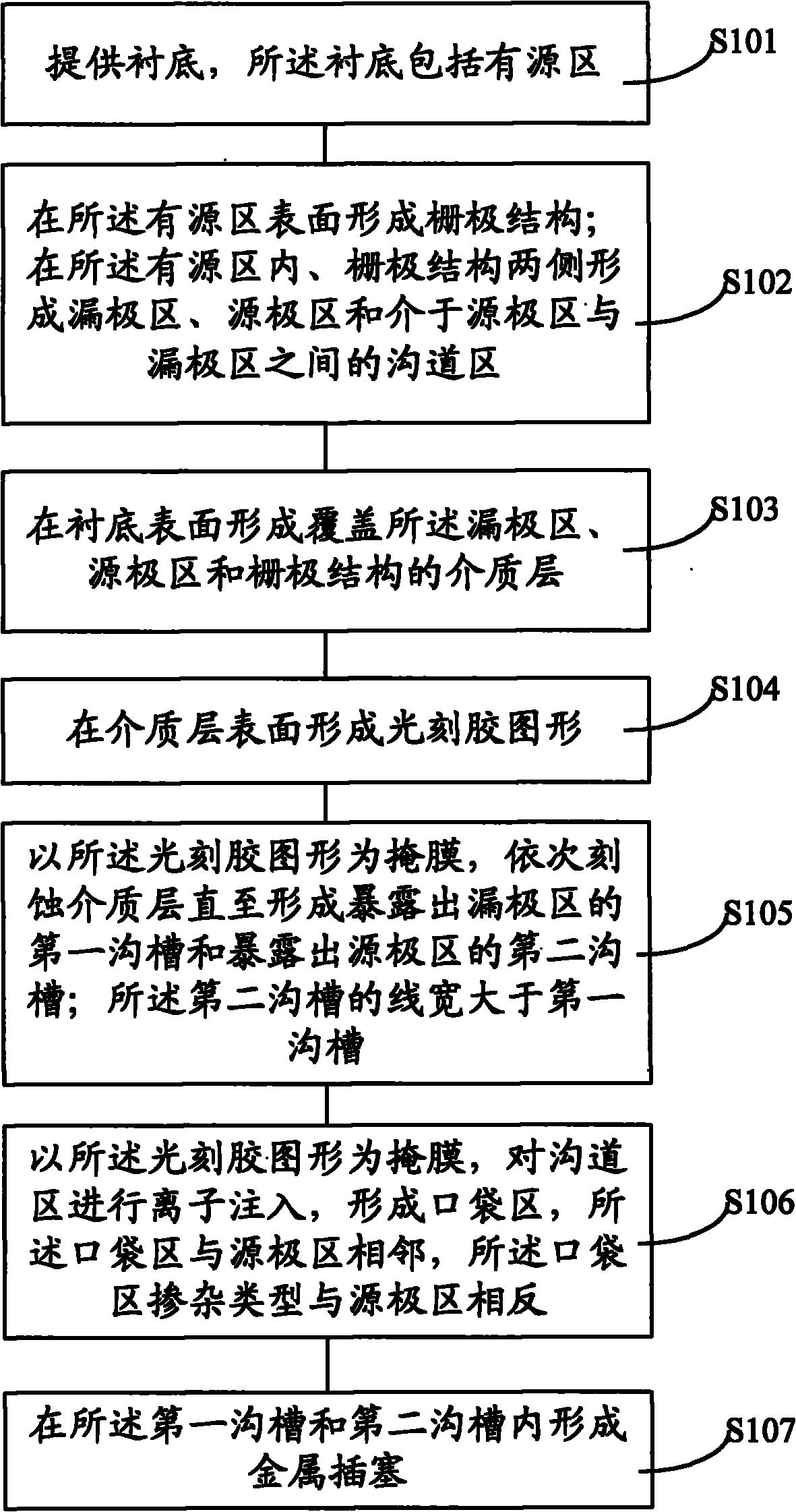
[0017] For this reason, the present invention provides a kind of forming method of asymmetric transistor, its flow process is as follows figure 2 As shown, it specifically includes the following steps:
[0018] Step S101, providing a substrate, the substrate including an active region;
[0019] Step S102, forming a gate ...
PUM
 Abstract
Description
Claims
Application Information