

Method for manufacturing lengthwise region of CoolMOS
A manufacturing method and vertical technology, applied in semiconductor/solid-state device manufacturing, electrical components, circuits, etc., can solve problems such as complex process, high processing cost, and long process time, so as to overcome voids, improve process efficiency, and improve process overly complex effects
- Summary
- Abstract
- Description
- Claims
- Application Information
AI Technical Summary
Problems solved by technology
Method used
Image

Examples
Embodiment Construction
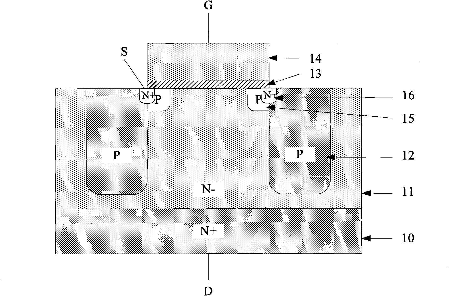
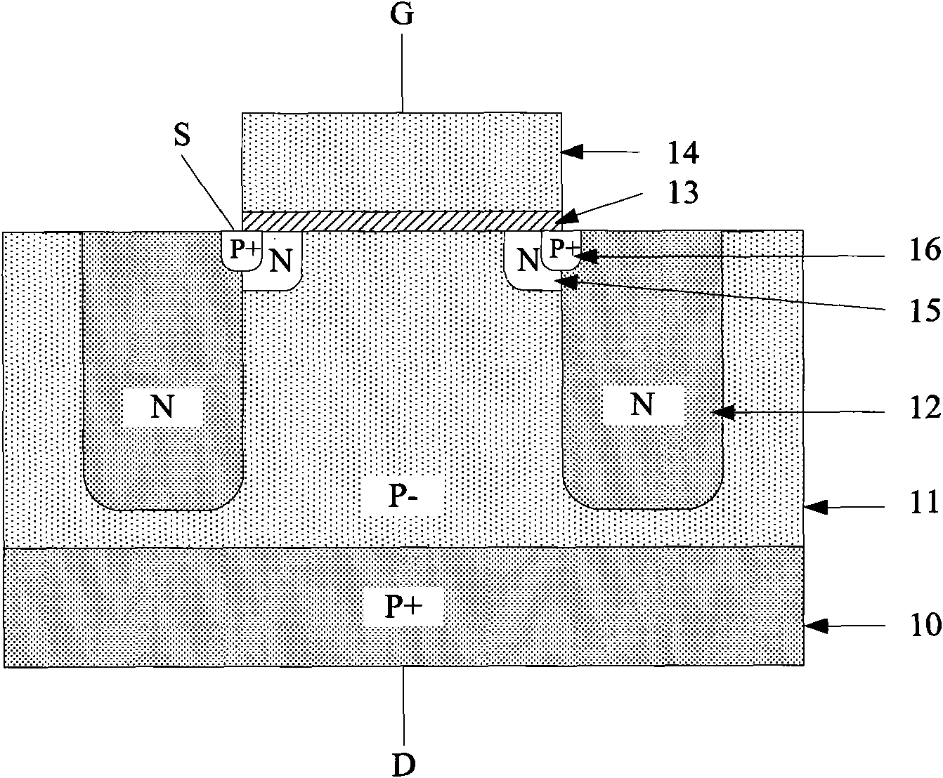
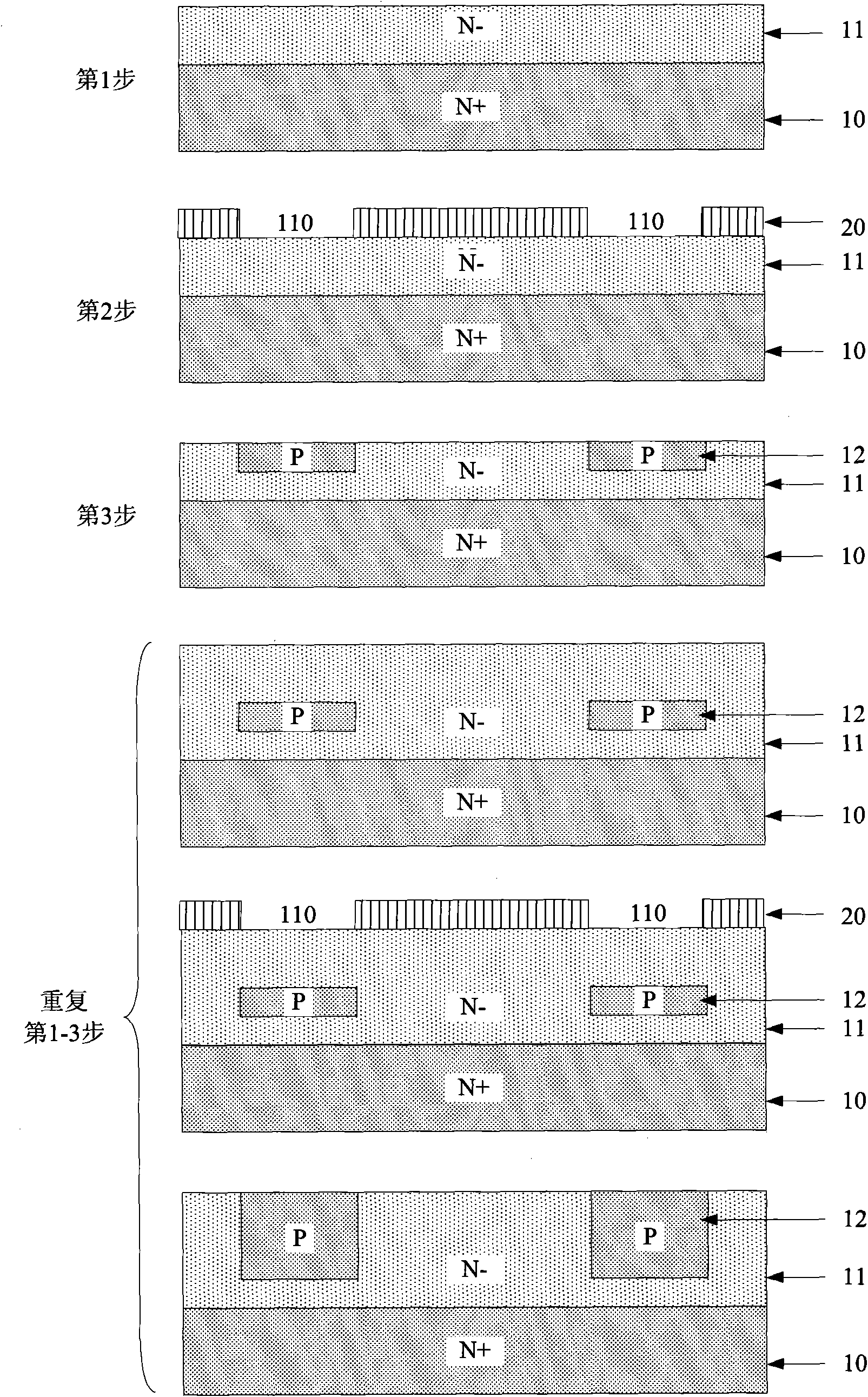
[0036] Taking the CoolMOS device based on PMOS as an example, the manufacturing method of CoolMOS of the present invention includes the following steps:
[0037] In the first step, a lightly doped N-type epitaxial layer 11 is grown on the heavily doped N-type silicon substrate 10 by using an epitaxial process. The epitaxial process is to deposit a single crystal layer on a single crystal substrate, usually using chemical vapor deposition (CVD) equipment.
[0038] In the second step, an ion implantation window 110 is defined on the epitaxial layer 11 by using a photolithography process, and the position of the ion implantation window 110 is the position of the P-type vertical region of the CoolMOS device. The so-called definition of the ion implantation window 110 means that after the photoresist 20 is coated on the silicon wafer, the photoresist 20 above the ion implantation window 110 is removed through steps such as exposure and development, and the photoresist 20 in the rem...
PUM
 Abstract
Description
Claims
Application Information