Supercharge Your Innovation With Domain-Expert AI Agents!

Silicon on insulator (SOI) wafer and formation method thereof

A technology of wafers and single crystal silicon wafers, which is applied in the field of SOI wafers and their formation, can solve the problems of reducing the insulation performance of the insulating layer, damage to the lattice of single crystal silicon wafers, and high production costs, and achieve simple process, high quality, and low production costs. low effect

Active Publication Date: 2011-03-30
XIAN YISHEN OPTOELECTRONICS TECH CO LTD
View PDF2 Cites 10 Cited by
  • Summary
  • Abstract
  • Description
  • Claims
  • Application Information

AI Technical Summary

Problems solved by technology

[0006] The three existing methods for forming SOI wafers all have certain defects: after the oxygen injection and annealing process in the oxygen injection isolation technology, the crystal lattice of the single crystal silicon wafer will be destroyed, which greatly reduces the insulation performance of the insulating layer. This in turn reduces the quality of the SOI material
[0007] In the "bonded SOI" technology, the silicon substrate with a thickness of about several hundred microns should be uniformly polished or etched to a few microns or even 1 micron or less, which is technically in terms of controllability and uniformity. It is very difficult, and the production cost is very high; in addition, in the process of bonding to form SOI, if there are contaminants in the bonding surface or unevenness due to the poor flatness of the bonding surface, there will be pores Occurs at the bonding interface, affecting the quality of SOI wafers
[0008] "Smart Cut" technology requires high process precision, making production difficult and costly

Method used


Image

  • Silicon on insulator (SOI) wafer and formation method thereof
  • Silicon on insulator (SOI) wafer and formation method thereof
  • Silicon on insulator (SOI) wafer and formation method thereof

Examples


Embodiment Construction

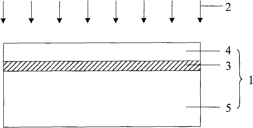
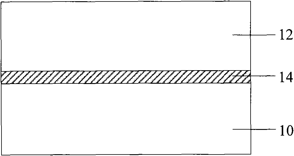
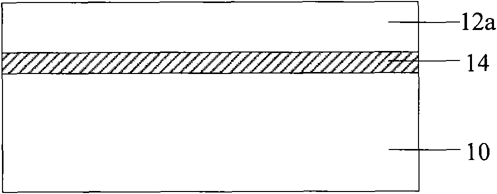
[0031] Several existing methods for manufacturing SOI wafers either cause damage to the crystal lattice of a single crystal silicon wafer, affecting the insulation capability of the SOI wafer, or have complex processes, high manufacturing costs, and poor quality of the formed SOI wafer. Embodiments of the present invention form grooves and cavities in the single crystal silicon wafer, and then form an insulating layer and an insulating material layer in the grooves and cavities as the insulating layer of the SOI wafer, and the insulating material layer in the cavities is made of single crystal silicon Slices are separated into silicon base and top silicon. The insulating silicon oxide of this process is formed by deposition or spin coating process, which not only solves the problem that the oxygen injection and annealing process in the oxygen injection isolation technology destroy the crystal lattice of the single crystal silicon wafer and reduce the insulation performance of t...


PUM


Abstract

The invention relates to a silicon on insulator (SOI) wafer and a formation method thereof, wherein the formation method of the SOI wafer comprises the following steps: providing a monocrystalline silicon chip on which a mask layer is formed; etching the mask layer and the monocrystalline silicon chip to form a plurality of grooves; forming first insulating layers on the side walls and bottoms ofthe grooves; etching to remove the first insulating layers on the bottoms of the grooves; etching the monocrystalline silicon chip under the grooves along the grooves to form holes; treating the inner walls of the holes to form second insulating layers; and filling insulating material layers in the grooves and the hoes. The SOI wafer has simple process, low manufacturing cost and high quality, and is compatible with the manufacture procedure of the standard silicon CMOS process.

Description

technical field [0001] The invention relates to the technical field of semiconductors, in particular to an SOI wafer and a forming method thereof. Background technique [0002] Currently, SOI (Silicon on Insulator, silicon on insulator) wafers are widely regarded as semiconductor substrates that can improve the performance of semiconductor devices. The SOI wafer includes a silicon base, an insulating insulating layer, and a top silicon layer. Such a structure has the following advantages: (1) It can be used to manufacture large-scale integrated circuits with lines below 0.1 μm, thereby eliminating the need to manufacture such highly integrated circuits in bulk silicon. Various parasitic effects produced by the device; (2) can be used to manufacture high-speed and low-power semiconductor devices required by various pocket devices; (3) can be used to manufacture semiconductor devices that are resistant to nuclear radiation; (4) form MOS Partial isolation of devices improves t...

Claims


Application Information

Patent Timeline
Patent Type & Authority Applications(China)
IPC IPC(8): H01L21/762H01L23/00
CPCH01L21/76283H01L21/76254
Inventor 黄河
Owner XIAN YISHEN OPTOELECTRONICS TECH CO LTD
Features
  • R&D
  • Intellectual Property
  • Life Sciences
  • Materials
  • Tech Scout
  • Unparalleled Data Quality
  • Higher Quality Content
  • 60% Fewer Hallucinations
Learn More