Bipolar junction transistor and bipolar CMOS (Complementary Metal Oxide Semiconductor) integrated circuit as well as manufacturing method

A technology of bipolar junction type and manufacturing method, which is applied in the direction of transistor, semiconductor/solid-state device manufacturing, circuit, etc., can solve the unfavorable integration of bipolar process and CMOS process, and the large difference in the thickness of bipolar junction transistors. Achieve the effect of improving current voltage and frequency characteristics and reducing series resistance

Active Publication Date: 2012-07-25
SHANGHAI HUAHONG GRACE SEMICON MFG CORP
View PDF1 Cites 0 Cited by
  • Summary
  • Abstract
  • Description
  • Claims
  • Application Information

AI Technical Summary

Problems solved by technology

[0007] The invention solves the problem that the formation thickness of bipolar junction transistor and CMOS is relatively different in SOI-BiCMOS technology in the prior art, which is not conducive to the integration of bipolar technology and CMOS technology.

Method used


Image

  • Bipolar junction transistor and bipolar CMOS (Complementary Metal Oxide Semiconductor) integrated circuit as well as manufacturing method
  • Bipolar junction transistor and bipolar CMOS (Complementary Metal Oxide Semiconductor) integrated circuit as well as manufacturing method
  • Bipolar junction transistor and bipolar CMOS (Complementary Metal Oxide Semiconductor) integrated circuit as well as manufacturing method

Examples


Embodiment approach

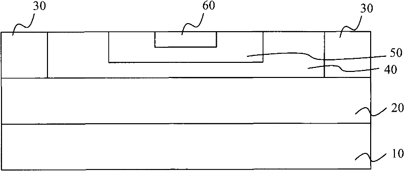
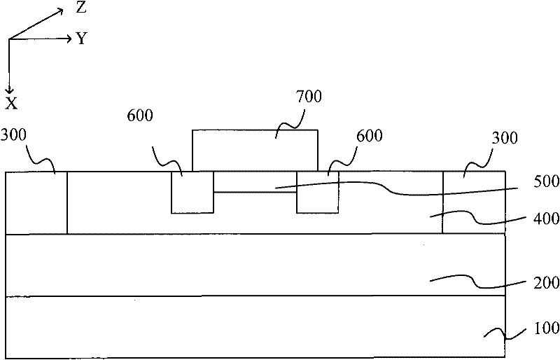
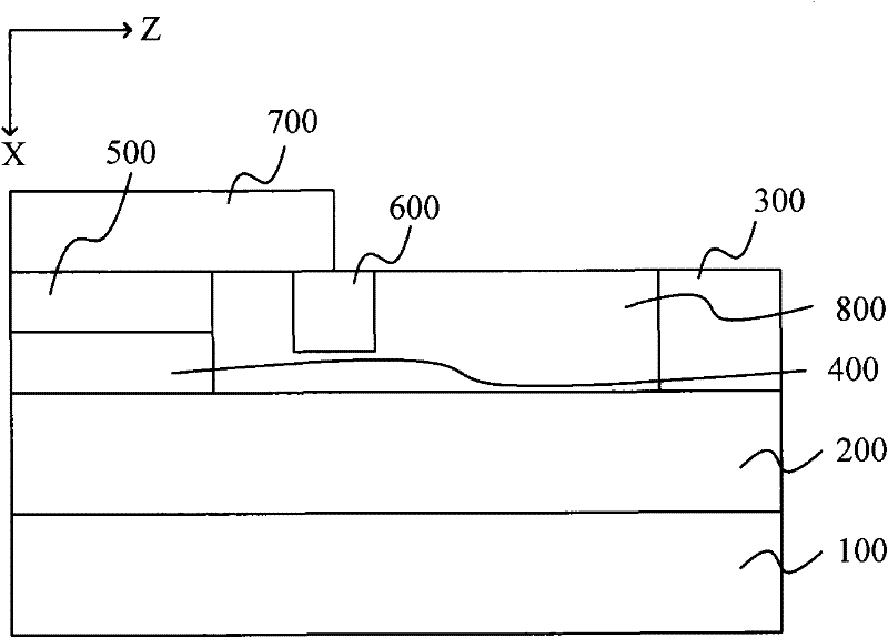
[0052] combine Figure 2a and Figure 2b As shown, an embodiment of the bipolar junction transistor of the present invention includes:

[0053] The first doped region 400 and the second doped region 800 adjacently distributed in the silicon-on-insulator substrate, and the first doped region 400 and the second doped region 800 are surrounded by a first isolation layer 300;

[0054] a third doped region 500 in the first doped region 400, the third doped region 500 is electrically connected to the second doped region 800;

[0055] A second isolation layer 600 surrounding the third doped region 500 in the first doped region 400 and the second doped region 800;

[0056] The doped polysilicon layer 700 on the third doped region 500 and the second isolation layer 600,

[0057] The doped polysilicon layer 700 , the third doped region 500 , and the first doped region 400 serve as the emitter region, the base region, and the collector region of the bipolar junction transistor, respec...


PUM


Abstract

The invention relates to a bipolar junction transistor and a bipolar CMOS (Complementary Metal Oxide Semiconductor) integrated circuit as well as a manufacturing method. The bipolar junction transistor comprises a first doped region, a second doped region, a third doped region in the first doped region, a second isolated layer in the first doped region and the second doped region and a doped polycrystalline silicon layer on the third doped region and the second isolated layer, wherein the first doped region and the second doped region are adjacent to be distributed on a silicon substrate of an insulator; the periphery of the first doped region and the second doped region is surrounded by a first isolated layer; the third doped region is electrically connected with the second doped region;the third doped region is surrounded by the second isolated layer; and the doped polycrystalline silicon layer, the third doped region and the first doped layer are respectively used as an emitter region, a base region and a collector region of the bipolar junction transistor. The bipolar junction transistor can be manufactured on a thin top silicon SOI (Silicon-On-Insulator) substrate so as to realize thin top silicon SOI-BiCMOS (Silicon-On-Insulator-Bipolar Complementary Metal Oxide Semiconductor) process integration.

Description

technical field [0001] The invention relates to the field of semiconductor manufacturing, in particular to a bipolar junction transistor (BJT, BipolarJunction Transistor), a bipolar CMOS (BiCMOS) integrated circuit and a manufacturing method. Background technique [0002] BiCMOS integrated circuit is an integrated circuit composed of bipolar gate circuit and CMOS gate circuit. At the same time, it has the characteristics of high density, low power consumption, high speed and large driving capacity. [0003] High-performance BiCMOS integrated circuits were proposed and implemented in the early 1980s. They are mainly used in high-speed static memories, high-speed gate arrays, and other high-speed digital circuits. They can also produce high-performance analog / digital hybrid circuits for system integration. [0004] The manufacturing process of BiCMOS can be mainly divided into two categories: BiCMOS process based on CMOS, and BiCMOS process based on bipolar process. [0005]...

Claims


Application Information

Patent Timeline
Patent Type & Authority Patents(China)
IPC IPC(8): H01L29/73H01L29/36H01L27/12H01L21/331H01L21/84
Inventor 周建华高明辉彭树根
Owner SHANGHAI HUAHONG GRACE SEMICON MFG CORP
Why Eureka
Try Eureka