
LED printed circuit board and preparation method of amorphous diamond heat dissipation and insulation film layer thereof

A technology of printed circuit board and amorphous diamond, which is applied in the direction of printed circuit manufacturing, printed circuit, printed circuit parts, etc., can solve the problems of poor heat dissipation effect of the electrical insulation layer, achieve improved heat dissipation effect, simplify the process, and simplify the process Effect

Inactive Publication Date: 2011-03-30
HARBIN INST OF TECH
View PDF4 Cites 7 Cited by
  • Summary
  • Abstract
  • Description
  • Claims
  • Application Information

AI Technical Summary

Problems solved by technology

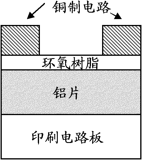
[0003] In order to solve the problem of poor heat dissipation effect of the electrical insulation layer of the existing LED printed circuit board, the present invention proposes a preparation method of the LED printed circuit board and its amorphous diamond heat dissipation insulating film layer

Method used


Image

  • LED printed circuit board and preparation method of amorphous diamond heat dissipation and insulation film layer thereof
  • LED printed circuit board and preparation method of amorphous diamond heat dissipation and insulation film layer thereof
  • LED printed circuit board and preparation method of amorphous diamond heat dissipation and insulation film layer thereof

Examples


specific Embodiment approach 1

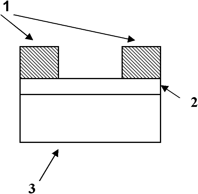
[0014] Specific implementation mode 1. Combination figure 2 Describe this embodiment mode, LED printed circuit board, it comprises printed circuit board 1, amorphous diamond heat dissipation insulating film layer 2, copper circuit layer 3, adds amorphous diamond heat dissipation between printed circuit board 1 and copper circuit layer 3 Insulation film layer 2.

specific Embodiment approach 2

[0015] Specific embodiment 2. This embodiment is a further description of specific embodiment 1. The amorphous diamond heat-dissipating insulating film layer 2 is sp rich sp deposited on the surface of the printed circuit board by using the filtered cathode vacuum arc system. 3 Hybrid amorphous diamond films.

specific Embodiment approach 3

[0016] Specific Embodiment 3. This embodiment is a further description of Specific Embodiment 1 or 2. The thickness of the amorphous diamond heat-dissipating insulating film layer 2 is 0.5-2 μm.


PUM

PropertyMeasurementUnit
Thicknessaaaaaaaaaa
Thicknessaaaaaaaaaa
Thermal conductivityaaaaaaaaaa

Abstract

The invention relates to a light-emitting diode (LED) printed circuit board and a preparation method of an amorphous diamond heat dissipation and insulation film layer thereof, in particular to an LED printed circuit board and a preparation method of a heat dissipation and insulation dual-efficacy film layer thereof. In the invention, the problem of poor heat dissipation effect of the existing LED printed circuit board because the hard-and-fast requirement of electric insulation is limited is solved, and an LED printed circuit board and a preparation method of an amorphous diamond heat dissipation and insulation film layer thereof are provided. The circuit board is formed by adding the amorphous diamond heat dissipation and insulation film layer between a printed circuit board and a copper circuit. The preparation method comprises the following concrete steps: (1) cleaning: cleaning the LED printed circuit board by deionized water, and blow-drying the LED printed circuit board; (2) etching: etching the amorphous diamond depositing surface of the LED printed circuit board by a Kaufman ion gun; and (3) depositing: alternately depositing carbon ions by adopting different negative bias to gradually form the heat dissipation and insulation dual-efficacy film layer of an amorphous diamond film formed by alternately constructing a sub-film layer with low stress and a sub-film layer with high sp3 hybridization content. The invention is suitable for printed circuit boards.

Description

technical field [0001] The invention relates to a thermal insulation double-effect film layer of an LED printed circuit board and a preparation method thereof. Background technique [0002] Semiconductor LED light source is known as the "fourth generation of energy-saving and environmentally friendly lighting source" after incandescent lamps, fluorescent lamps and high-intensity discharge lamps (HID). It leads the third lighting revolution and is called the light source of the 21st century. The emergence of LED has brought mankind into a new era of green and environmentally friendly lighting. As the carrier of the LED electronic circuit system, the role of the printed circuit board is very important in the entire solid-state lighting system. However, the heat dissipation effect of the current LED printed circuit board is greatly limited due to the requirement of electrical insulation. Once the heat dissipation effect of the printed circuit board is not good, the temperatur...

Claims


Application Information

Patent Timeline
IPC IPC(8): H05K1/02H05K3/00F21V29/00F21Y101/02F21V29/508F21V29/85
Inventor 韩杰才朱嘉琦刘罡王扬何玉荣
Owner HARBIN INST OF TECH
Learn More