Annealing apparatus

An annealing device and annealing treatment technology, applied in electrical components, semiconductor/solid-state device manufacturing, circuits, etc., can solve the problems of unbalanced and uneven temperature distribution, and achieve the effect of high energy conversion efficiency

Inactive Publication Date: 2011-03-30
TOKYO ELECTRON LTD
View PDF3 Cites 3 Cited by
  • Summary
  • Abstract
  • Description
  • Claims
  • Application Information

AI Technical Summary

Problems solved by technology

However, since the heating light is monochromatic light (single wavelength), there is a problem of unbalanced (non-uniform) temperature distribution due to the structure or surface state of the wafer surface to be heated.

Method used


Image

  • Annealing apparatus
  • Annealing apparatus
  • Annealing apparatus

Examples


Embodiment Construction

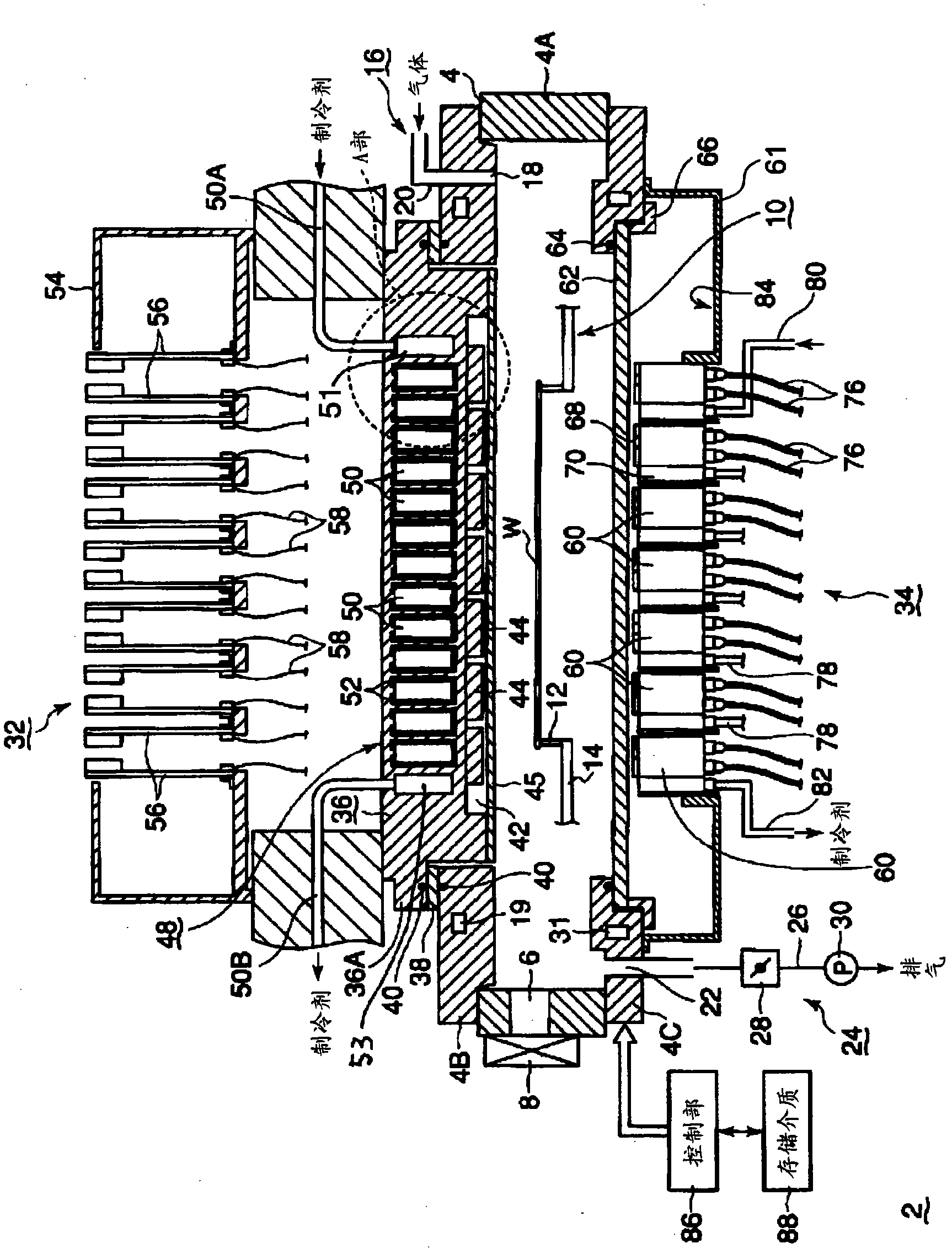
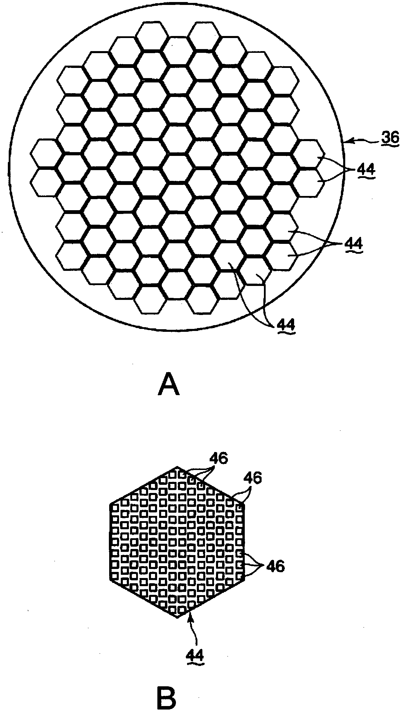
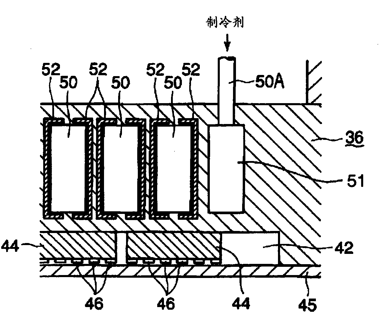
[0052] Hereinafter, one embodiment of the annealing apparatus of the present invention will be described in detail based on the drawings.figure 1 It is a cross-sectional view showing a schematic configuration of an embodiment of the annealing apparatus of the present invention. figure 2 A is a plan view showing the surface (lower surface) of the surface-side heating mechanism. figure 2 B is a partial enlarged plan view of the surface (lower surface) of the surface-side heating mechanism. image 3 is indicated as part of the heating mechanism on the surface side figure 1 An enlarged cross-sectional view of part A in . Figure 4 It is a plan view showing the surface (upper surface) of the rear side heating mechanism. Figure 5 It is an explanatory diagram for explaining the light emitting state of a semiconductor laser element. Figure 6 It is a schematic diagram showing the irradiation state of laser light (heating light) from a laser element. Here, as an object to be pro...


PUM


Abstract

Provided is an annealing apparatus which anneals a subject to be processed. The annealing apparatus is provided with: a processing container wherein the subject to be processed is stored; a supporting means which supports the subject to be processed in the processing chamber; a gas supply means which supplies a processing gas into the processing container; an air-releasing means which releases the atmosphere from the processing container; and a rear-side heating means having a plurality of laser elements which radiate heating light toward the entire rear surface of the subject to be processed.

Description

technical field [0001] The present invention relates to an annealing apparatus for annealing an object to be processed such as a semiconductor wafer, and more particularly to an annealing apparatus for annealing by irradiating heating light from a laser element or an LED (Light Emitting Diode) element. Background technique [0002] Generally, in order to manufacture a semiconductor integrated circuit, various processes such as film formation, oxidation diffusion, modification, etching, and annealing are repeatedly performed on semiconductor wafers such as silicon substrates. Among these treatments, in the annealing treatment for activating impurity atoms doped in the wafer after ion plating, it is necessary to increase and decrease the temperature of the semiconductor wafer at a higher speed in order to minimize the diffusion of impurities. [0003] In a conventional annealing apparatus, a wafer is heated using a halogen lamp or the like. However, it takes at least about 1 ...

Claims


Application Information

Patent Timeline
Patent Type & Authority Applications(China)
IPC IPC(8): H01L21/268H01L21/26H01L21/265
CPCH01L21/67115
Inventor 铃木智博米田昌刚河西繁大矢和广
Owner TOKYO ELECTRON LTD
Why Eureka
Try Eureka