Tunneling field effect transistor with T-shaped grid structure and low power consumption

A tunneling field effect, transistor technology, applied in semiconductor devices, electrical components, circuits, etc., can solve the problems of complexity, increased cost, process complexity, insufficient drive current, etc., achieve high on-current, and improve subthreshold slope. , Improve the effect of conduction current

Active Publication Date: 2011-12-28
SEMICONDUCTOR MANUFACTURING INTERNATIONAL (BEIJING) CORP +1
View PDF0 Cites 0 Cited by
  • Summary
  • Abstract
  • Description
  • Claims
  • Application Information

AI Technical Summary

Problems solved by technology

At present, the main challenge encountered by TFET is that the driving current is not enough due to the influence of tunneling current.
At present, the main methods to increase the conduction current of TFET are: (1) Thinning the thickness of the gate dielectric layer, increasing the dielectric constant of the gate dielectric layer and improving the gate control ability. This method uses high-K dielectrics compared to growing silicon dioxide gate dielectrics. The process is relatively complex, and due to the influence of gate leakage, the thickness of the dielectric layer also has a limit value; (2) use narrow bandgap semiconductor materials to reduce the width of the tunneling barrier and increase the tunneling current. This method is due to the introduction of other Semiconductor materials undoubtedly increase the cost and process complexity

Method used


Image

  • Tunneling field effect transistor with T-shaped grid structure and low power consumption
  • Tunneling field effect transistor with T-shaped grid structure and low power consumption
  • Tunneling field effect transistor with T-shaped grid structure and low power consumption

Examples


Embodiment Construction

[0021] The present invention will be further described below by example. It should be noted that the purpose of the disclosed embodiments is to help further understand the present invention, but those skilled in the art can understand that various replacements and modifications are possible without departing from the spirit and scope of the present invention and the appended claims of. Therefore, the present invention should not be limited to the content disclosed in the embodiments, and the protection scope of the present invention is subject to the scope defined in the claims.

[0022] The invention can be prepared completely by adopting the conventional TFET process flow, and the key part is the layout structure of the grid.

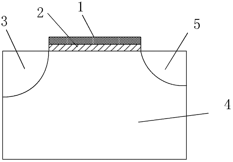
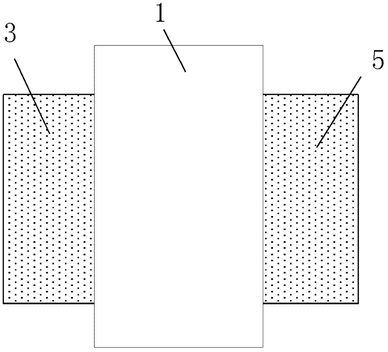
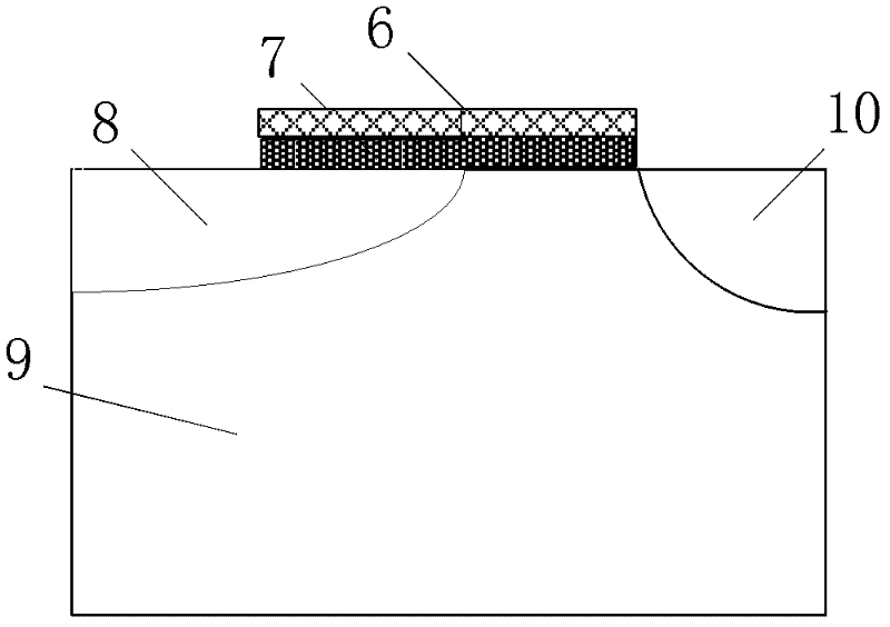
[0023] The specific implementation steps are shown in Figure 3:

[0024] 1. Grow the gate oxide layer 7 on the substrate 9. The smaller the gate thickness, the better the gate control capability of the device. The ideal value is about 4nm-20nm, and ...


PUM


Abstract

The invention provides a tunneling field effect transistor (TFET) with a T-shaped grid structure and low power consumption, and belongs to the field of field effect transistor logic devices and circuits in complementary metal oxide semiconductor (CMOS) ultra large scale integrated circuits (ULSI). The TFET comprises a source electrode, a drain electrode and a control grid, wherein the control grid extends toward the end of the source electrode to form a T shape; the T-shaped control grid consists of an extending grid region and the original control grid region; and an active region covered below the extending grid region is a channel region and is made of a substrate material. By using the T-shaped grid structure, the source region of the TFET encircles a channel, so that the conduction current of a device is improved. Compared with the conventional planar TFET, the TFET can achieve higher conduction current and steeper subthreshold slope under the same process conditions and the samesize of the active region.

Description

technical field [0001] The invention belongs to the field of field effect transistor logic devices and circuits in CMOS ultra large integrated circuits (ULSI), in particular to a tunneling field effect transistor (TFET). Background technique [0002] As the size of the device continues to shrink, the negative impact of the short channel effect of the device is increasing. DIBL (drain-to-barrier lowering effect) and band-band tunneling effect make the off-state leakage current of the device continuously increase. Not only that, the subthreshold slope of traditional MOSFET devices cannot be reduced synchronously with the reduction of device size due to the theoretical limitation of KT / q. Therefore, with the decrease of the threshold voltage of the device, the subthreshold leakage current is also increasing continuously. Today, the resulting static power consumption has become the focus of everyone's attention in small-size devices. In order to break through the theoretical ...

Claims


Application Information

Patent Timeline
Patent Type & Authority Patents(China)
IPC IPC(8): H01L29/78H01L29/423
Inventor 詹瞻黄芊芊黄如王阳元
Owner SEMICONDUCTOR MANUFACTURING INTERNATIONAL (BEIJING) CORP
Why Eureka
Try Eureka