Comb-shaped gate composite source MOS (Metal Oxide Semiconductor) transistor and manufacturing method thereof

A technology of MOS transistors and source regions, applied in semiconductor/solid-state device manufacturing, semiconductor devices, electrical components, etc., can solve the problems of low on-state current, low leakage current, small on-state current, etc., and reduce the leakage current problem , low leakage current, and the effect of reducing parasitic resistance

Active Publication Date: 2011-07-06
SEMICONDUCTOR MANUFACTURING INTERNATIONAL (BEIJING) CORP +1
View PDF6 Cites 6 Cited by
  • Summary
  • Abstract
  • Description
  • Claims
  • Application Information

AI Technical Summary

Problems solved by technology

TFET has many excellent characteristics such as low leakage current, low sub-threshold slope, low operating voltage and low power consumption. However, due to the limitation of source junction tunneling probability and tunneling area, TFET faces low open current problem
The patent (CN101719517A) proposes a Schottky tunneling transistor, which solves the source-drain self-alignment problem of TFET devices by using the Schottky junction in the source-drain, but it also faces the problem of small on-state current

Method used


Image

  • Comb-shaped gate composite source MOS (Metal Oxide Semiconductor) transistor and manufacturing method thereof
  • Comb-shaped gate composite source MOS (Metal Oxide Semiconductor) transistor and manufacturing method thereof
  • Comb-shaped gate composite source MOS (Metal Oxide Semiconductor) transistor and manufacturing method thereof

Examples


Embodiment Construction

[0043] The present invention will be further described below by example. It should be noted that the purpose of the disclosed embodiments is to help further understand the present invention, but those skilled in the art can understand that various replacements and modifications are possible without departing from the spirit and scope of the present invention and the appended claims of. Therefore, the present invention should not be limited to the content disclosed in the embodiments, and the protection scope of the present invention is subject to the scope defined in the claims.

[0044] A specific example of the production method of the present invention includes Figure 1 to Figure 5b Process steps shown:

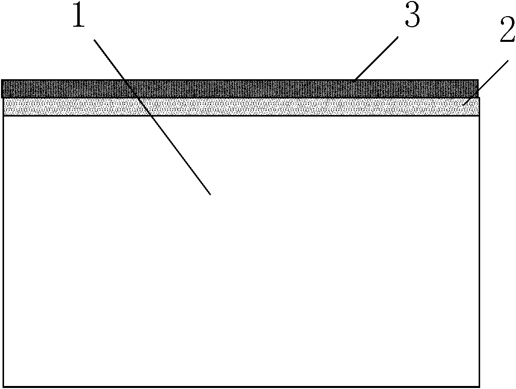
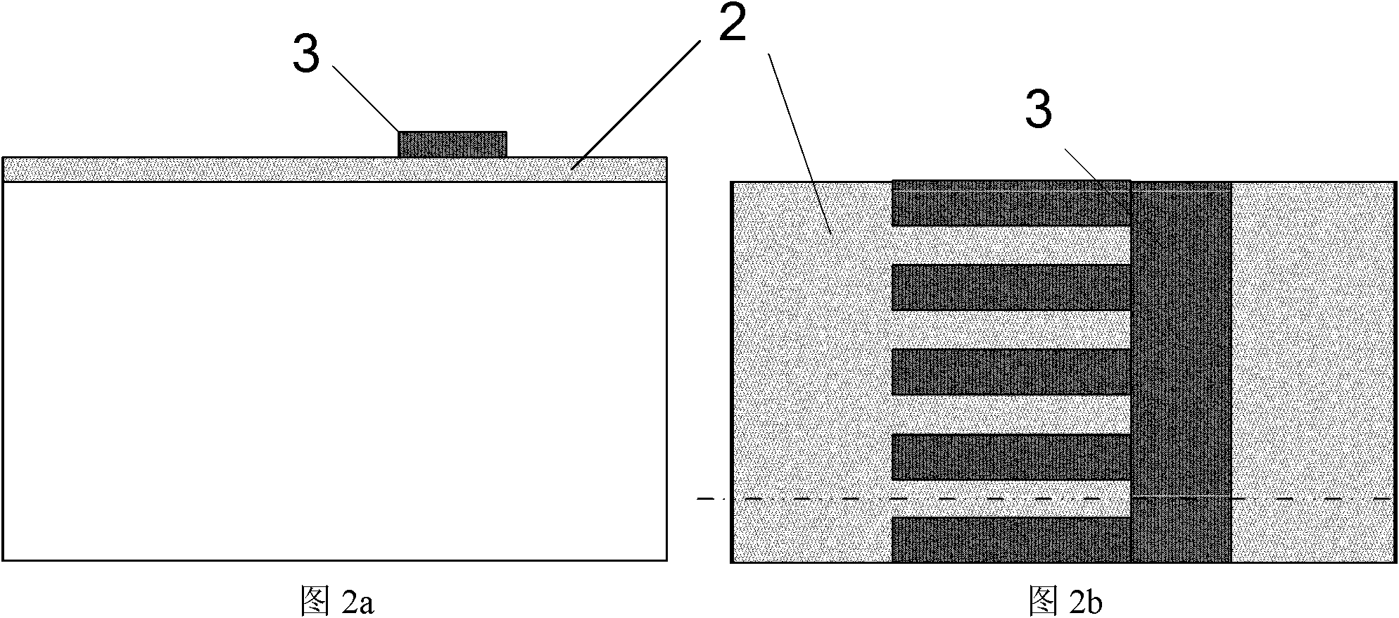
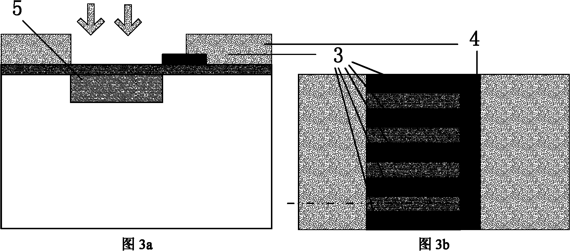
[0045] 1. Fabricate an active region isolation layer on a bulk silicon wafer silicon substrate 1 with a crystal orientation of (100) using shallow trench isolation technology, and the doping concentration of the substrate is lightly doped; then thermally grow a gate die...


PUM


Abstract

The invention provides a composite source MOS (Metal Oxide Semiconductor) transistor with schottky barrier and comb-shaped gate structures and a manufacturing method thereof. The composite source MOS transistor comprises a control gate electrode layer, a gate dielectric layer, a semiconductor substrate, a high doped source region and a high doped drain region, wherein one side far away from the channel direction of the high doped source region is connected with a schottky source region; one end of a control gate extends towards the high doped source region; the extended gate region is an extension gate shaped like a comb; the original control gate region is a main gate; the active region covered by the extension gate is likewise a channel region with the substrate material; the high doped source region is formed by the high doping of semiconductor and is located on the two sides of each comb of the extension gate; and a schottky junction is formed at the channel under the schottky source region and the extension gate. Compared with the traditional MOSFET (Metal-Oxide-Semiconductor Field Effect Transistor), the composite source MOS transistor can obtain a higher conduction current, a lower leakage current and a steeper subthreshold slope under a same technological condition and a same active region size.

Description

technical field [0001] The invention belongs to the field of field effect transistor logic devices and circuits in CMOS ultra large integrated circuits (ULSI), and in particular relates to a composite source MOS transistor combined with a Schottky barrier (Schottky Barrier) and a comb gate structure and a manufacturing method thereof. Background technique [0002] As the size of metal-oxide-silicon field-effect transistors (MOSFETs) continues to shrink, especially when the feature size of the device enters the nanoscale, the negative impact of the short channel effect of the device becomes more and more obvious. Drain-induced barrier-lowering effect (DIBL) and band-band tunneling effect increase the off-state leakage current of the device, which increases the power consumption of the integrated circuit along with the decrease of the threshold voltage of the device. Not only that, the subthreshold slope of traditional MOSFET devices cannot be reduced synchronously with the re...

Claims


Application Information

Patent Timeline
Patent Type & Authority Applications(China)
IPC IPC(8): H01L29/78H01L29/423H01L21/336
CPCH01L29/78H01L29/7839H01L29/423H01L29/4238
Inventor 黄芊芊詹瞻黄如王阳元
Owner SEMICONDUCTOR MANUFACTURING INTERNATIONAL (BEIJING) CORP
Why Eureka
Try Eureka