Back drilling method of through via, circuit board and manufacturing method of circuit board

A manufacturing method and circuit board technology, applied in the directions of printed circuit manufacturing, circuits, printed circuits, etc., can solve the problem that the digital receiver is difficult to determine whether it is received or not, and achieve the effect of reducing back-drilling errors and excellent performance.

Inactive Publication Date: 2011-04-06
UNIMICRON TECH SHEN ZHEN
View PDF5 Cites 15 Cited by
  • Summary
  • Abstract
  • Description
  • Claims
  • Application Information

AI Technical Summary

Problems solved by technology

These blanking pulses close the eye, making it more difficult for a digital receiver to determine whether it is receiving a logic 1 or a logic 0 signal

Method used


Image

  • Back drilling method of through via, circuit board and manufacturing method of circuit board
  • Back drilling method of through via, circuit board and manufacturing method of circuit board
  • Back drilling method of through via, circuit board and manufacturing method of circuit board

Examples


Embodiment Construction

[0035] The content disclosed in this application does not limit the subject matter of this application or the detailed description of this application. The subject matter of the application is set forth in the detailed description of the application and in the appended claims. Other aspects of the subject matter of the present application will be obvious to those of ordinary skill in the art after reading and understanding the following detailed description and referring to the accompanying drawings, and will not constitute a limitation to the present invention in a certain sense.

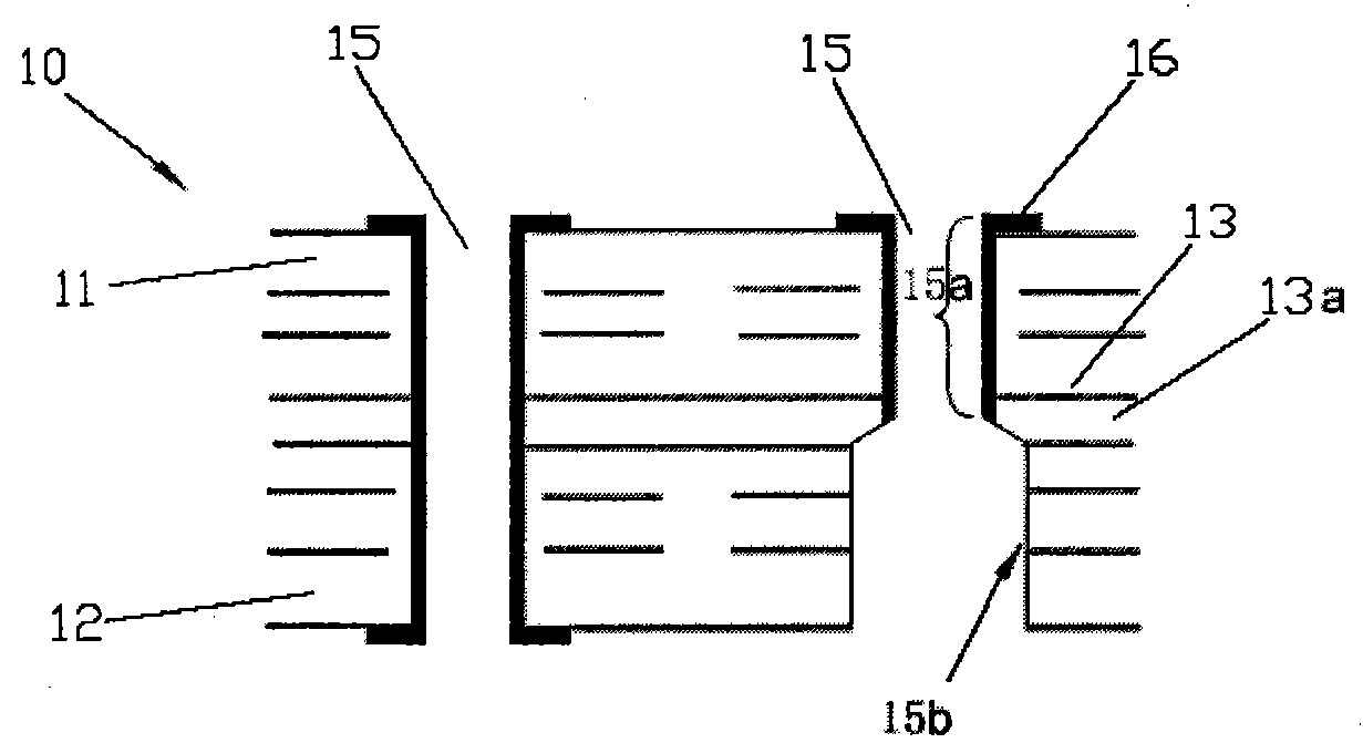
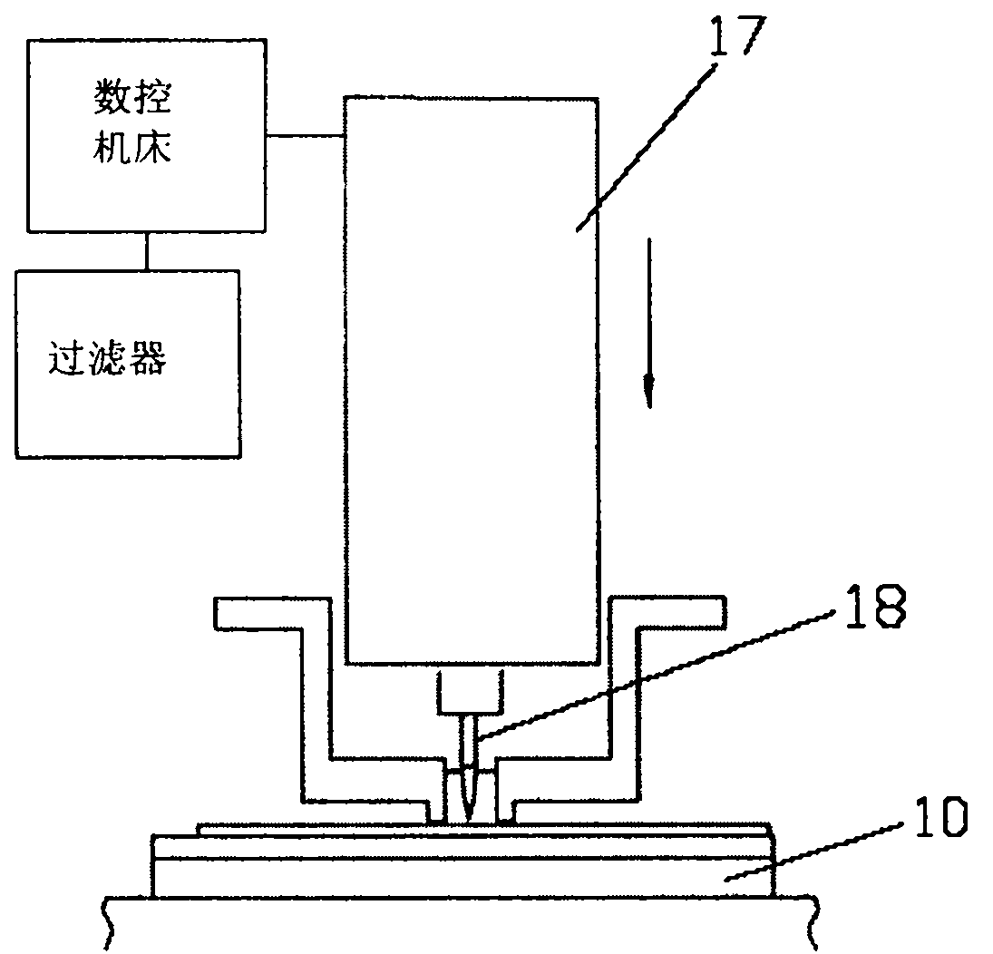
[0036] Please refer to Figure 5 , Figure 5 A flowchart showing the backdrilling method of the via hole of the present invention. The back drilling method comprises the following steps:

[0037] Step S01: using a drilling machine to measure the local thickness of the circuit board with the target through hole at the target through hole;

[0038] Step S02: automatically determine the back-drill...


PUM


Abstract

A back-drilling method of through vias in a circuit board is disclosed. The back-drilling method comprises the steps of: using a drill machine for measuring a localized thickness of the circuit board at a location having a target through via; determining a back drill depth at the location to be back-drilled according to the measured localized thickness and a predetermined percentage; and back-drilling the target through via to the determined depth, thereby forming a back-drilled via extending to a preselected target layer, wherein the percentage is verified by a cross-sectional slice mode, and the slice method comprises the steps of: selecting slices at a plurality of locations to be backdrilled; measuring total thickness of the circuit board at the plurality of locations and layer depths of the target layer at the plurality of locations; and obtaining the percentage based on layer depth of the target layer and the total thickness of the circuit board at the plurality of locations.

Description

technical field [0001] The present invention relates to circuit board manufacturing technology, in particular to a through-hole back-drilling method for removing selected parts, a circuit board and a method for manufacturing the circuit board. Background technique [0002] For decades, circuit boards, especially printed circuit boards (PCBs), have been widely used to support and electrically connect selected electronic components. Printed circuit boards typically include copper for electrical connections separated by an electrically insulating dielectric material. Connections between layers are often made through vias or plated through holes (PTHs). Generally, to realize the electrical connection between layers, it is necessary to drill through holes, such as plated through holes, from the top to the bottom of the selected layer in the vertical direction. [0003] With the advent of wireless digital communication technologies, such as wireless networks, mobile phones, GPS ...

Claims


Application Information

Patent Timeline
Patent Type & Authority Applications(China)
IPC IPC(8): H05K3/42H05K1/11H01L21/48B32B38/04
CPCH05K2203/0242H05K2203/0207H05K3/429H05K1/0251H05K3/0047
Inventor 爱克特·泰佛勒斯
Owner UNIMICRON TECH SHEN ZHEN
Why Eureka
Try Eureka