Supercharge Your Innovation With Domain-Expert AI Agents!

TFT-LCD drive power and bias circuit

A technology of bias circuit and drive power supply, which is applied in the electronic field, and can solve problems such as increased electromagnetic interference noise, peak voltage generation, drive system voltage, and bias circuit stability and quality degradation, so as to improve stability and improve stability and the effect of EMC characteristics

Active Publication Date: 2011-04-20
SHANGHAI TIANMA MICRO ELECTRONICS CO LTD
View PDF0 Cites 5 Cited by
  • Summary
  • Abstract
  • Description
  • Claims
  • Application Information

AI Technical Summary

Problems solved by technology

As mentioned above, these peak voltages lead to a decrease in the stability and quality of the driving system voltage and bias circuit of the entire TFT-LCD, affecting the display quality and electromagnetic compatibility (EMC) characteristics of the entire product
[0012] Therefore, there are at least the following problems in the prior art: the existing TFT-LCD driving power supply and bias circuit will produce peak voltage, thereby causing an increase in electromagnetic interference noise, affecting the driving system voltage of the entire TFT-LCD and the stability and stability of the bias circuit. Electromagnetic compatibility characteristics

Method used


Image

  • TFT-LCD drive power and bias circuit
  • TFT-LCD drive power and bias circuit
  • TFT-LCD drive power and bias circuit

Examples


Embodiment 1

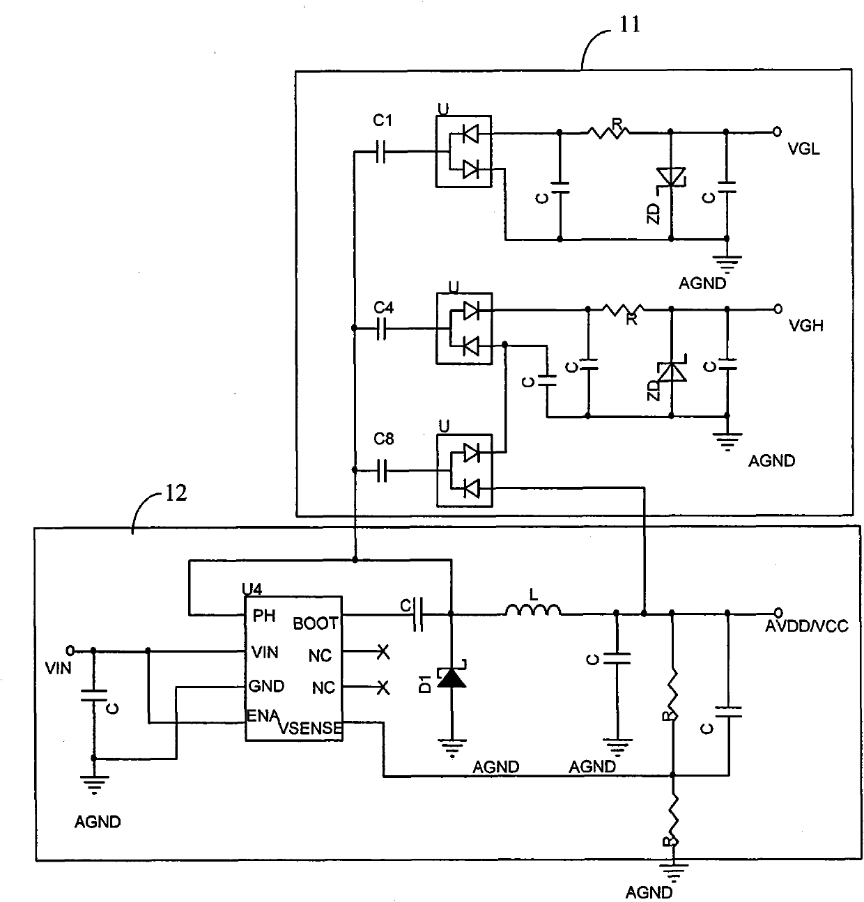
[0059] Please see Figure 7 , Figure 7 It is a schematic diagram of a TFT-LCD driving power supply and a bias circuit according to the first embodiment of the present invention. In this embodiment, the switching regulated power supply circuit is a step-down switching regulated power supply circuit 71, the switching regulated power supply is a step-down switching regulated power supply U4, and the first pulse width modulation voltage output terminal is The pulse width modulation voltage output terminal PH of the step-down switching power supply U4, the first noise suppression element can be a high-frequency high-impedance element such as the first inductor L2, a magnetic bead, a resistor, or a certain length of wire.

[0060] Preferably, when the first noise suppression element is the first inductor L2 and the frequency of the step-down switching regulated power supply U4 is 1 MHz, the value range of the first inductor L2 is 0.5 μH-3.0 μH. Such as Figure 7 As shown, the TF...

Embodiment 2

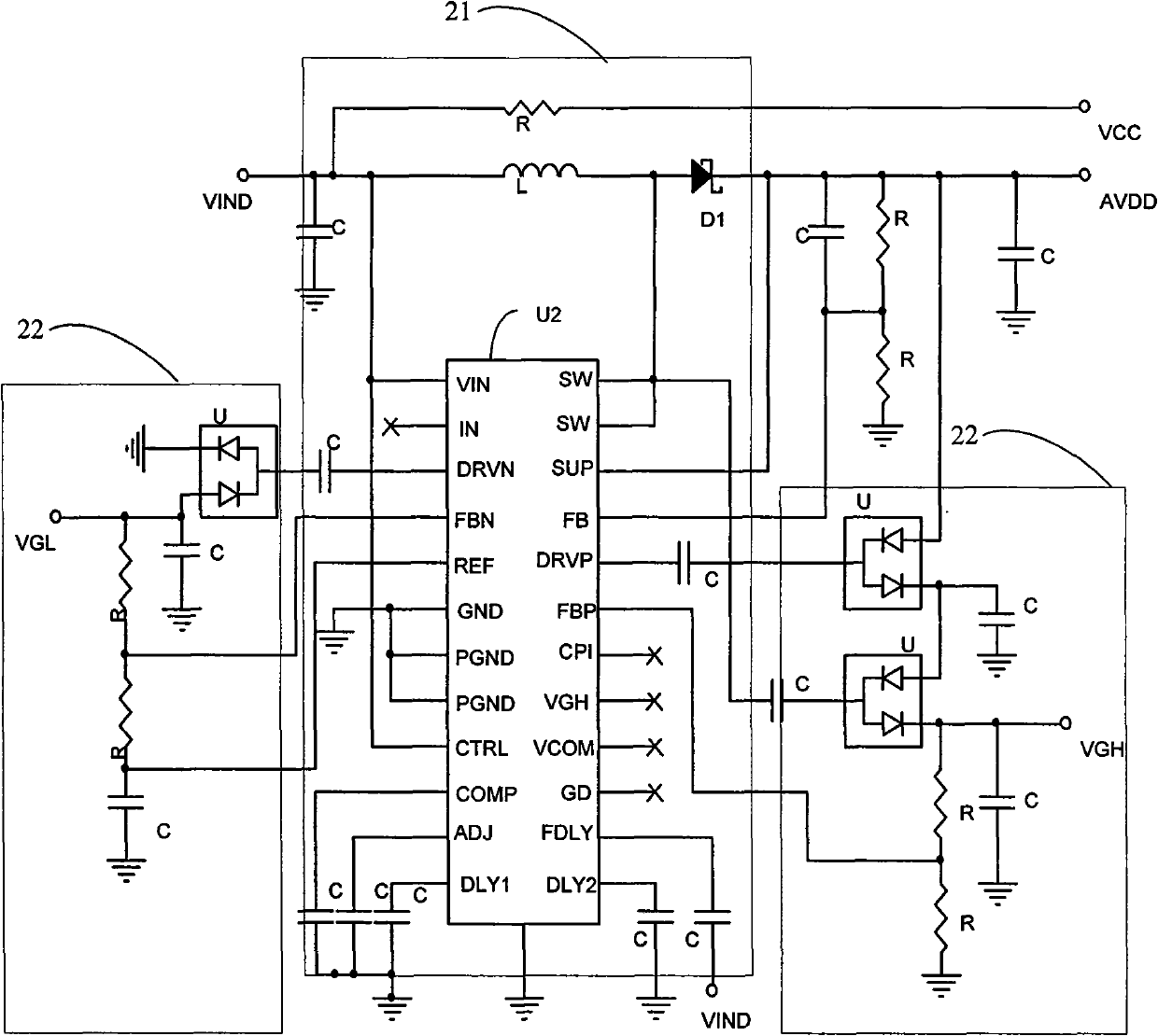
[0085] read on Figure 12 , is a schematic diagram of the TFT-LCD drive power supply and bias circuit according to the second embodiment of the present invention.

[0086] In this embodiment, the switch regulated power supply circuit is a step-up switch regulated power supply circuit 110, the switch regulated power supply is a step-up switch regulated power supply U2, and the first pulse width modulation voltage output terminal can be It is the adjustable pulse width modulation voltage output terminal SW, the negative pulse width modulation voltage output terminal DRVN or the positive pulse width modulation voltage output terminal DRVP of the step-up switching regulated power supply U2, and the second pulse width modulation voltage is a negative pulse width The modulation voltage output terminal DRVN or the positive pulse width modulation voltage output terminal DRVP, the first noise suppression element can be a first inductor L2, a magnetic bead, a resistor or a wire of a cer...


PUM


Abstract

The invention provides a thin film transistor liquid crystal display (TFT-LCD) drive power and bias circuit. The TFT-LCD drive power and bias circuit comprises a switch voltage-stabilized source circuit and a charge pump circuit, wherein the switch voltage-stabilized source circuit comprises a switch voltage-stabilized source which is provided with a first pulse width modulation voltage output end; the charge pump circuit is provided with a first bias input end; and a first noise suppression element is connected between the first pulse width modulation voltage output end and the first bias input end. The technical scheme provided by the invention can effectively prevent spike voltage noise on a pulse width modulation voltage signal from being coupled to drive power and bias voltage through a way provided by a capacitor, so that the driving system voltage, bias circuit stability and electromagnetic compatibility of the whole TFT-LCD can be improved.

Description

technical field [0001] The present invention relates to the field of electronic technology, in particular to a thin film transistor liquid crystal display (Thinfilm transistor liquid crystal display, TFT-LCD) drive power supply and bias circuit. Background technique [0002] TFT-LCD driving power supply and bias circuit generate driving power such as digital power supply voltage (VCC), analog power supply voltage (AVDD), and bias voltage such as gate turn-on voltage (VGH, TFT Gate ON Power), gate turn-off voltage ( VGL, TFT Gate OFF Power) and other voltages are provided to the liquid crystal display or liquid crystal module. Therefore, the TFT-LCD driving power supply and bias circuit are indispensable parts of the liquid crystal display or liquid crystal module driving circuit. direct impact. [0003] The TFT-LCD driving power supply and bias circuit are mainly composed of a step-down or boost switching regulated power supply circuit (Buck or Boost Switcher Regulator) an...

Claims


Application Information

Patent Timeline
Patent Type & Authority Applications(China)
IPC IPC(8): G09G3/36
Inventor 沈岭
Owner SHANGHAI TIANMA MICRO ELECTRONICS CO LTD
Features
  • R&D
  • Intellectual Property
  • Life Sciences
  • Materials
  • Tech Scout
  • Unparalleled Data Quality
  • Higher Quality Content
  • 60% Fewer Hallucinations
Learn More