

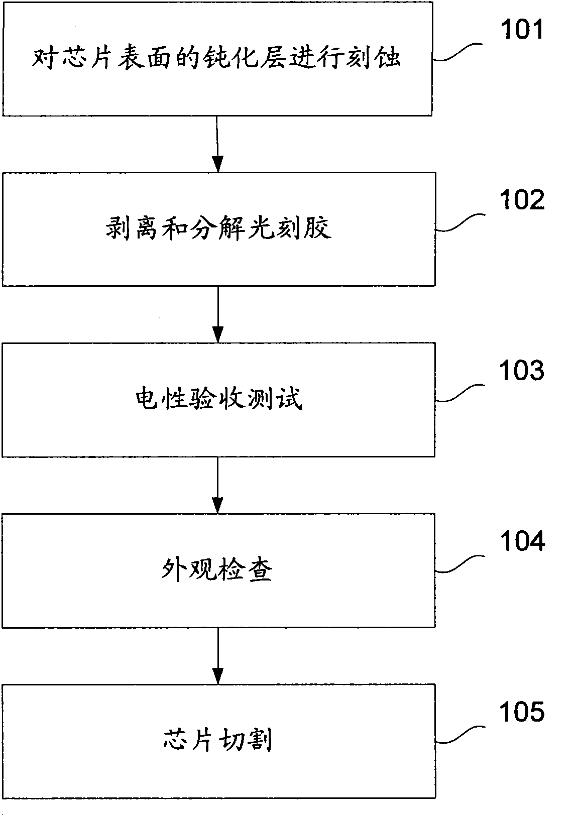
Method for improving chip cutting
A chip and cutting process technology, which is applied in the field of integrated circuit chip cutting, can solve problems such as chip characteristic influence, chip failure, etc., and achieve the effects of improving quality and output, reducing pollution, and suppressing effects
- Summary
- Abstract
- Description
- Claims
- Application Information
AI Technical Summary
Problems solved by technology
Method used
Image

Examples
Embodiment Construction
[0024] In the following description, numerous specific details are given in order to provide a more thorough understanding of the present invention. It will be apparent, however, to one skilled in the art that the present invention may be practiced without one or more of these details. In other examples, some technical features known in the art are not described in order to avoid confusion with the present invention.
[0025] In order to thoroughly understand the present invention, detailed steps will be presented in the following description to illustrate how the present invention reduces the contamination of the bonding pads by improving the chip dicing method. Obviously, the practice of the invention is not limited to specific details familiar to those skilled in the semiconductor arts. Preferred embodiments of the present invention are described in detail below, however, the present invention may have other embodiments besides these detailed descriptions.
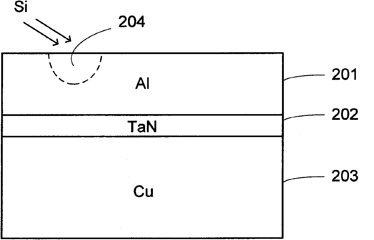
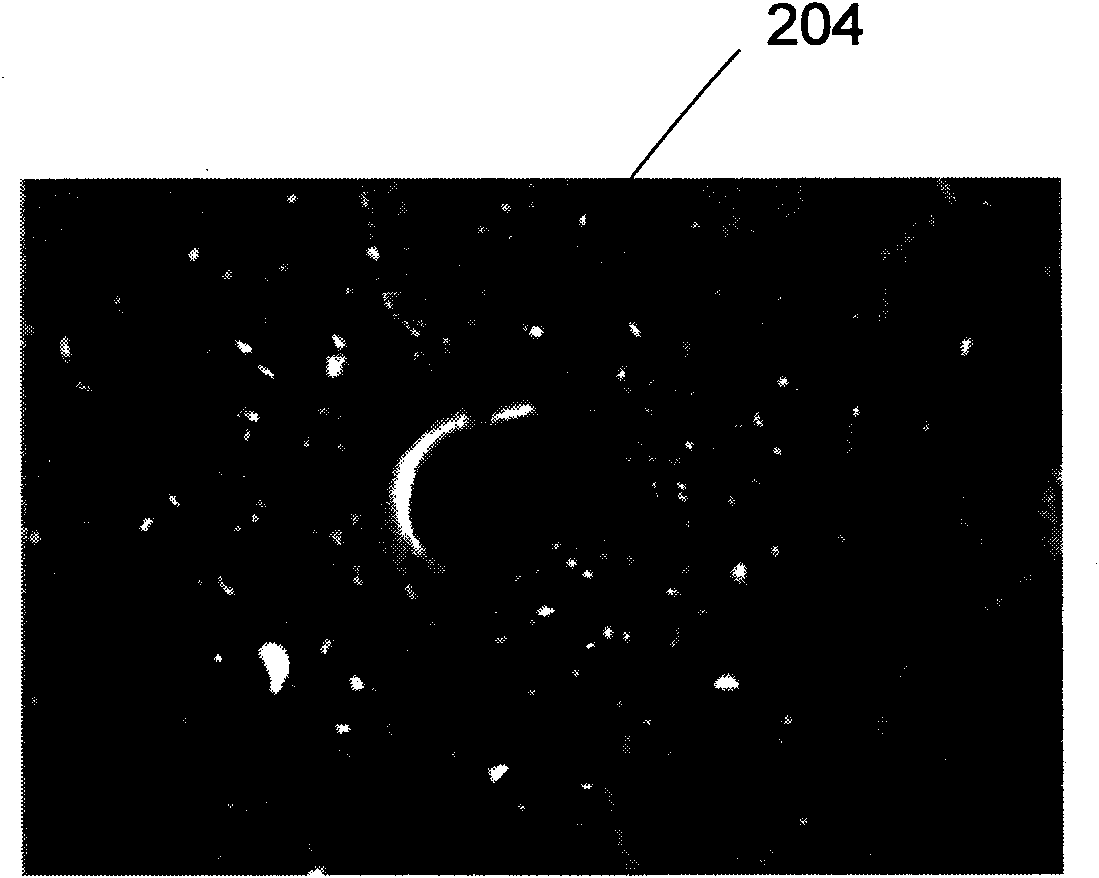
[0026] refer ...
PUM
| Property | Measurement | Unit |
|---|---|---|
| Thickness | aaaaa | aaaaa |
| Thickness | aaaaa | aaaaa |
Abstract
Description
Claims
Application Information