Contact pad

A technology for contact pads and pads, which is applied to electrical components, electrical solid devices, circuits, etc., can solve the problems of reducing parasitic capacitance, limited height, etc., and achieve good isolation effect.

Active Publication Date: 2011-04-20
SHANGHAI HUAHONG GRACE SEMICON MFG CORP
View PDF0 Cites 6 Cited by
  • Summary
  • Abstract
  • Description
  • Claims
  • Application Information

AI Technical Summary

Problems solved by technology

[0005] Through research, it is found that the STI region of the prior art that reduces parasitic capacitance has obvious disadvantages: since the formation of the shallow trench isolation layer requires a CMP (Chemical Mechanical Planarization, chemical mechanical planarization) process to complete, because the CMP has a castellation (Disshing ) effect, it is generally not easy

Method used


Image

  • Contact pad
  • Contact pad
  • Contact pad

Examples


Embodiment Construction

[0022] In order to make the above objects, features and advantages of the present invention more comprehensible, the embodiments of the present invention will be further described in detail below in conjunction with the accompanying drawings and specific implementation methods.

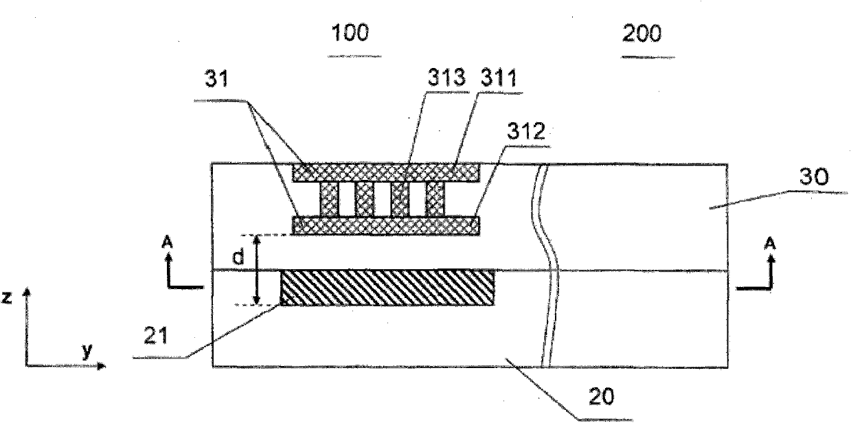
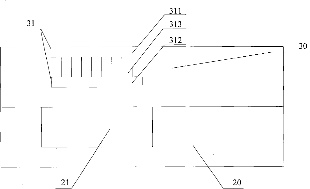
[0023] figure 2 Shown is a schematic diagram of a contact pad structure provided by the present invention in order to reduce the parasitic capacitance in the CMOS device. Such as figure 2 As shown, the contact pad is formed in the substrate 20 and the interconnect structure layer 30, wherein the Z direction is a direction perpendicular to the upper surface of the semiconductor substrate. The interconnect structure layer 30 includes a multi-layer metal layer, and the contact pad includes a pad metal layer 31. In this embodiment, the pad metal layer 31 includes a first layer of pad metal layer 311, a second layer of pad metal layer 312 and A hole 313 for connecting the first layer of pad metal layer...


PUM


Abstract

A contact pad belongs to protection circuit design field of semiconductor integrated circuit. The contact pad provided by the present invention comprises a pad metal layer, and further comprises a totally depleted layer area formed by simultaneously neutralizing and doping a first type trap and a second type trap for an active region; the totally depleted layer area is located under the pad metal layer and formed at an upper surface layer of a semiconductor substrate. Compared with the prior art, the totally depleted layer area increases a distance between an upper electrode and a lower electrode of the parasitic capacitance of the contact pad, reduces the value of the parasitic capacitance; simultaneously, the preparation of the totally depleted layer area can use the ion implantation of existing art, wherein the operation is simple and extra processes are not needed.

Description

technical field [0001] The invention relates to the field of protection circuit design of semiconductor integrated circuits, in particular to a contact pad. Background technique [0002] In the packaging technology field of semiconductor manufacturing, after the integrated circuit is manufactured, the contact pad (Pad) formed on the surface of the interconnection structure layer is electrically connected to the internal circuit as the interface between the internal circuit and the external signal, usually by The bonding method is that the metal wire completes the electrical connection between the external circuit and the contact pad. [0003] At the same time, as the feature size of the chip continues to decrease, the speed of the chip is getting faster and faster, and the requirements for the parasitic capacitance of various structures are getting higher and higher. The smaller the parasitic capacitance, the better the operating speed and frequency characteristics of the ch...

Claims


Application Information

Patent Timeline
IPC IPC(8): H01L23/482H01L29/06
CPCH01L2924/0002
Inventor 何军
Owner SHANGHAI HUAHONG GRACE SEMICON MFG CORP
Why Eureka
Try Eureka