
Packaging structure used for integrating surface adhesive type assembly

A surface-mounted, packaged structure technology, applied in electrical components, electrical solid-state devices, semiconductor devices, etc., can solve the problems of increasing the volume of the circuit carrier, increasing the volume of the circuit carrier, and reducing the volume, etc., to improve the bonding strength. , Improve the matching between the characteristic impedance of the antenna and the impedance of the system end, and increase the effect of space utilization

Inactive Publication Date: 2011-04-20
胡泉凌
View PDF0 Cites 6 Cited by
  • Summary
  • Abstract
  • Description
  • Claims
  • Application Information

AI Technical Summary

Problems solved by technology

When the signal is transmitted on the circuit board, passive components (such as resistors, capacitors, inductors, etc.) can be used to eliminate noise and stabilize the circuit to improve the quality of signal transmission. In addition, in the wiring of the antenna line, passive components can also be used It is set for the purpose of electrical impedance matching and frequency adjustment, but the passive components are set on the surface of the circuit carrier, so that the volume of the circuit carrier increases and the purpose of reducing the volume cannot be achieved
In addition, with the diversification of the functions of electronic products, the volume of the circuit carrier board will become larger, and the purpose of lightness, thinness and shortness cannot be achieved.

Method used


Image

  • Packaging structure used for integrating surface adhesive type assembly
  • Packaging structure used for integrating surface adhesive type assembly
  • Packaging structure used for integrating surface adhesive type assembly

Examples


Embodiment Construction

[0052] In order to further have a clearer and more detailed understanding and understanding of the structure and features of the present invention, the novelty and other features of the present invention are illustrated with preferred embodiments, and detailed descriptions are as follows in conjunction with the drawings:

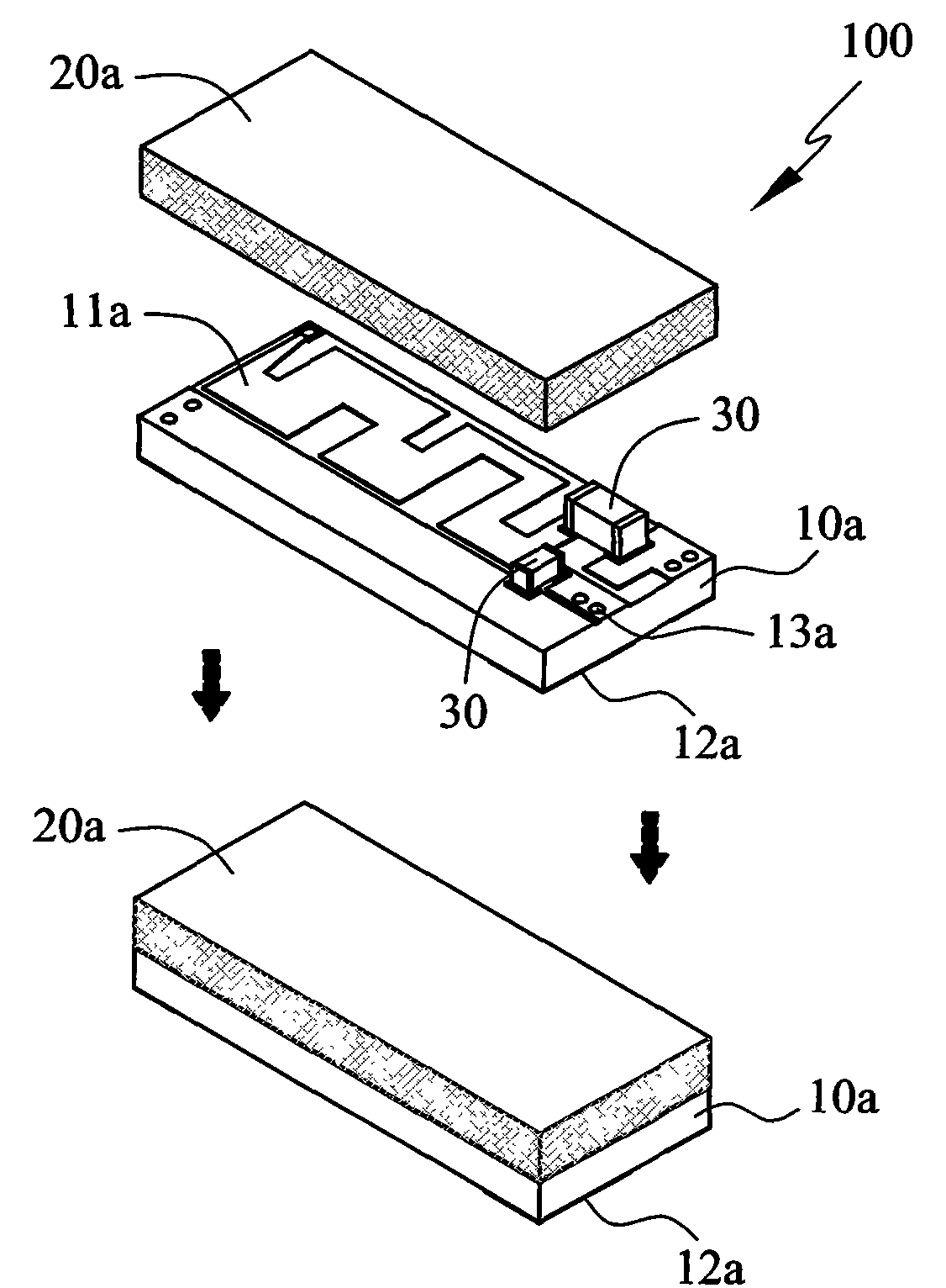
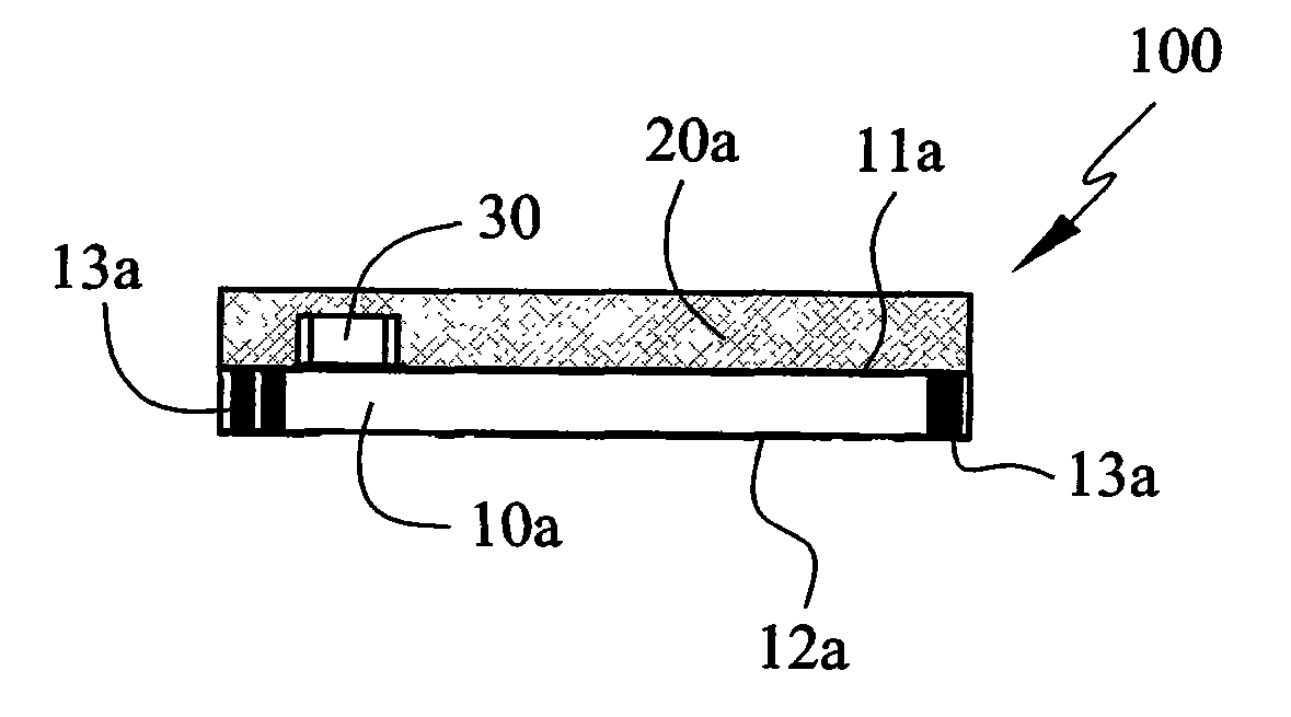
[0053] Please refer to figure 1 and figure 2 , which is the first preferred example of the present invention, the packaging structure (100) of the integrated surface mount type component includes: a dielectric substrate (10a), a first surface metal layer (11a), a second surface metal layer A layer (12a), a plurality of plated through holes (13a), a plurality of passive components (30), and an encapsulation rubber sheet (20a).

[0054] The dielectric substrate (10a) is a composite material composed of a dielectric resin and glass fiber or a composite material composed of a dielectric resin and a ceramic plate or ceramic powder, and the dielectric constant o...


PUM


Abstract

The present invention relates to a packaging structure used for integrating surface adhesive type assembly, which is used for integrating and packaging the surface adhesive type assemblies (such as a combination of an electronic assembly, a driving / driven assembly, a radio frequency module, an integrated circuit chip, a chip antenna or other surface adhesive type assemblies) by vacuum hot-pressing technology. The structure includes a dielectric substrate, a first surface metal layer arranged on a top surface of the dielectric substrate, a second surface metal layer arranged on an lower surface of the dielectric substrate, a plurality of plated-through-holes arranged in the dielectric substrate and used for electrically connecting the first surface metal layer and the second surface metal layer, an electronic assembly adhered to the first surface metal layer, and a packaging rubber sheet covered on the top surface of the dielectric substrate and used for sealing the first surface metal layer and the electronic assembly adhering thereto. The packaging structure used for integrating surface adhesive type assembly provides the function of bearing and structure protection, and ensures a normal transmission of signals and energy.

Description

technical field [0001] The present invention is an integrated packaging structure of surface-mounted components through vacuum thermocompression bonding technology, which provides the functions of bearing and structural protection, and ensures the transmission of signals and energy. Background technique [0002] With the rapid development of the semiconductor industry, future electronic products will emphasize the characteristics of thinness, shortness, high speed, high pin count, etc., and the traditional package type based on lead frame will gradually become unsuitable. Therefore, many challenges will be faced in the packaging process, such as packaging The selection of materials, the high-density accumulation of the number of gold wires in the packaging process, and the problems of gold wire offset and thin package warpage during mold flow filling are all problems encountered by the industry at present, and investment is required. the scope of the study. [0003] In conv...

Claims


Application Information

Patent Timeline
Patent Type & Authority Applications(China)
IPC IPC(8): H01L25/00H01L23/498H01L23/12H01L21/48
CPCH01L2224/45124H01L2924/3011H01L2924/30107H01L2224/48091H01L2224/48227H01L2224/49171H01L2924/15311H01L2924/19105H01L2924/30111
Inventor 胡泉凌杨成发林舜天
Owner 胡泉凌
Learn More