

Semiconductor device and manufacturing method thereof
A manufacturing method and semiconductor technology, which are applied in the manufacturing of semiconductor/solid-state devices, semiconductor devices, semiconductor/solid-state device components, etc., can solve problems such as defects, wiring short circuits, etc., and achieve the effect of improving oxidation resistance and reliability.
Active Publication Date: 2015-08-05
FUJITSU LTD
View PDF7 Cites 0 Cited by
- Summary
- Abstract
- Description
- Claims
- Application Information
AI Technical Summary
Problems solved by technology
If copper diffuses in the interlayer insulating film, there is a possibility of causing wiring short circuit or wiring failure, etc.
Method used
View moreImage
Smart ImageViewing Examples

Examples
Embodiment 1
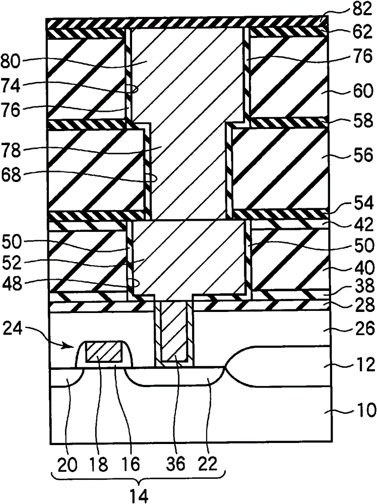
[0123]Using the above manufacturing process, a semiconductor device using β-SiC with a film thickness of 5 nm as the barrier layers 50 and 76 was manufactured.
Embodiment 2
[0125] Using the above manufacturing process, a semiconductor device using β-SiC with a film thickness of 10 nm as the barrier layers 50 and 76 was manufactured.
Embodiment 3
[0127] Using the above manufacturing process, a semiconductor device using ?-SiC with a film thickness of 20 nm as the barrier layers 50, 76 was manufactured.
Login to View More PUM
| Property | Measurement | Unit |
|---|---|---|
| elastic modulus | aaaaa | aaaaa |
| thickness | aaaaa | aaaaa |
| thickness | aaaaa | aaaaa |
Abstract
The method of manufacturing a semiconductor device includes forming an insulating film of a silicon compound-group insulation film; forming an opening in the insulation film, applying an active energy beam in an atmosphere containing hydrocarbon gas to form a barrier layer of a crystalline SiC, and forming an interconnection structure of copper in the opening with the barrier layer formed in.
Description
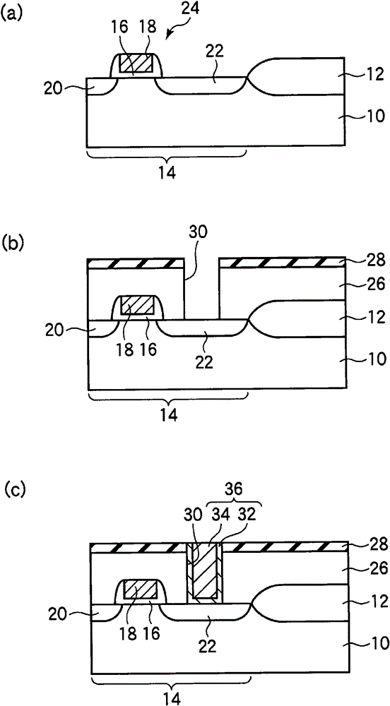
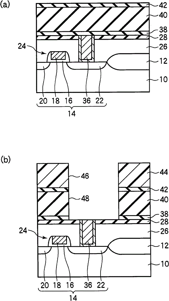
technical field [0001] The present invention relates to a semiconductor device and its manufacturing method, and more particularly to a semiconductor device including copper wiring and its manufacturing method. Background technique [0002] Along with the demand for miniaturization and high performance of semiconductor devices, in the formation of wiring layers of semiconductor devices in recent years, a so-called damascene process is adopted, that is, after forming groove patterns and hole patterns on the interlayer insulating film, then Grooves and holes are embedded with wiring material. As a wiring material, copper (Cu) is used as a material having lower resistance instead of conventional aluminum. [0003] Copper is a metal material that is easily diffused in a silicon oxide film that is a main material of an interlayer insulating film. If copper diffuses in the interlayer insulating film, there is a possibility of causing a wiring short circuit, wiring failure, or th...
Claims
Login to View More Application Information
Patent Timeline
 Patent Type & AuthorityPatents(China)
IPC IPC(8): H01L21/768H01L21/316H01L23/522
CPCH01L23/53238H01L21/76826H01L21/76831H01L21/76829H01L23/485H01L21/76825H01L21/02203H01L21/02282H01L23/53295H01L21/3105H01L21/31695H01L21/76807H01L2924/0002H01L21/02126H01L21/02274H01L2924/00
Inventor尾崎史朗中田义弘小林靖志美浓浦优一
OwnerFUJITSU LTD