

Preparation method of observation sample of device insulated isolation region for transmission electron microscope
An electron microscope, insulation isolation technology, used in semiconductor/solid-state device testing/measurement, instruments, measuring devices, etc., can solve problems such as affecting accurate measurement
- Summary
- Abstract
- Description
- Claims
- Application Information
AI Technical Summary
Problems solved by technology
Method used
Image

Examples
Embodiment Construction
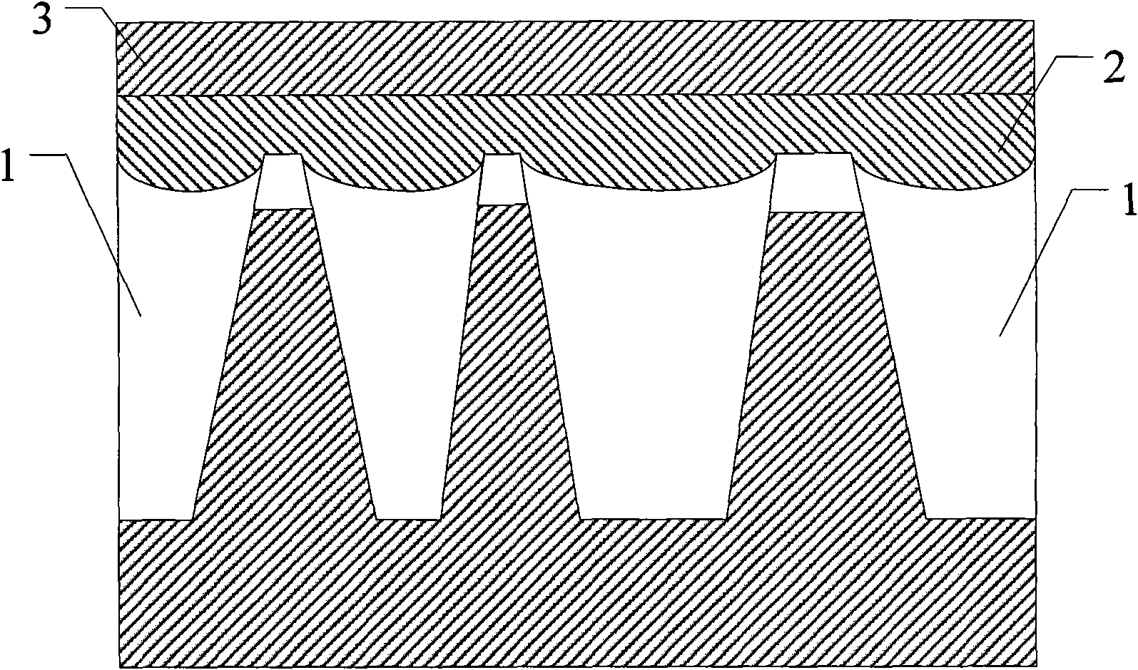
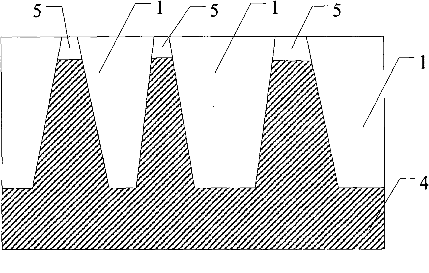
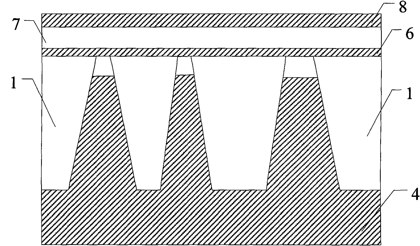
[0021] In order to make the above objects, features and advantages of the present invention more comprehensible, specific implementations of the present invention will be described in detail below in conjunction with the accompanying drawings.
[0022] A method for preparing a sample preparation method for observation of a device insulation isolation region for a transmission electron microscope can be realized in a variety of alternative ways, and the following is illustrated by a preferred embodiment. Of course, the present invention is not limited to this specific method. Examples, general replacements known to those skilled in the art undoubtedly fall within the protection scope of the present invention.
[0023] Secondly, the present invention is described in detail using schematic diagrams. When describing the embodiments of the present invention in detail, for the convenience of illustration, the schematic diagrams are not partially enlarged according to the general scal...
PUM
| Property | Measurement | Unit |
|---|---|---|
| Thickness | aaaaa | aaaaa |
| Thickness | aaaaa | aaaaa |
| Thickness | aaaaa | aaaaa |
Abstract
Description
Claims
Application Information