Multilayer wiring board

A wiring substrate and wiring technology, which is applied in the manufacture of multilayer circuits, high-current matching devices, waveguides, etc. problems such as transmission of frequency signals to achieve high installation density, suppress the deterioration of transmission signals, and achieve the effect of high density

Inactive Publication Date: 2011-05-11
TOHOKU UNIV +1
View PDF6 Cites 10 Cited by
  • Summary
  • Abstract
  • Description
  • Claims
  • Application Information

AI Technical Summary

Problems solved by technology

[0003] However, since the high frequency of the signal frequency and the high density of the signal wiring increase the transmission loss, it is difficult to ensure the reliability of the transmitted signal, so that it is impossible to solve the problem of high density of the signal wiring on the same substrate. and issues of transmission of high-frequency signals

Method used


Image

  • Multilayer wiring board
  • Multilayer wiring board
  • Multilayer wiring board

Examples


no. 1 approach

[0043] Next, a first embodiment of the present invention will be described based on the drawings.

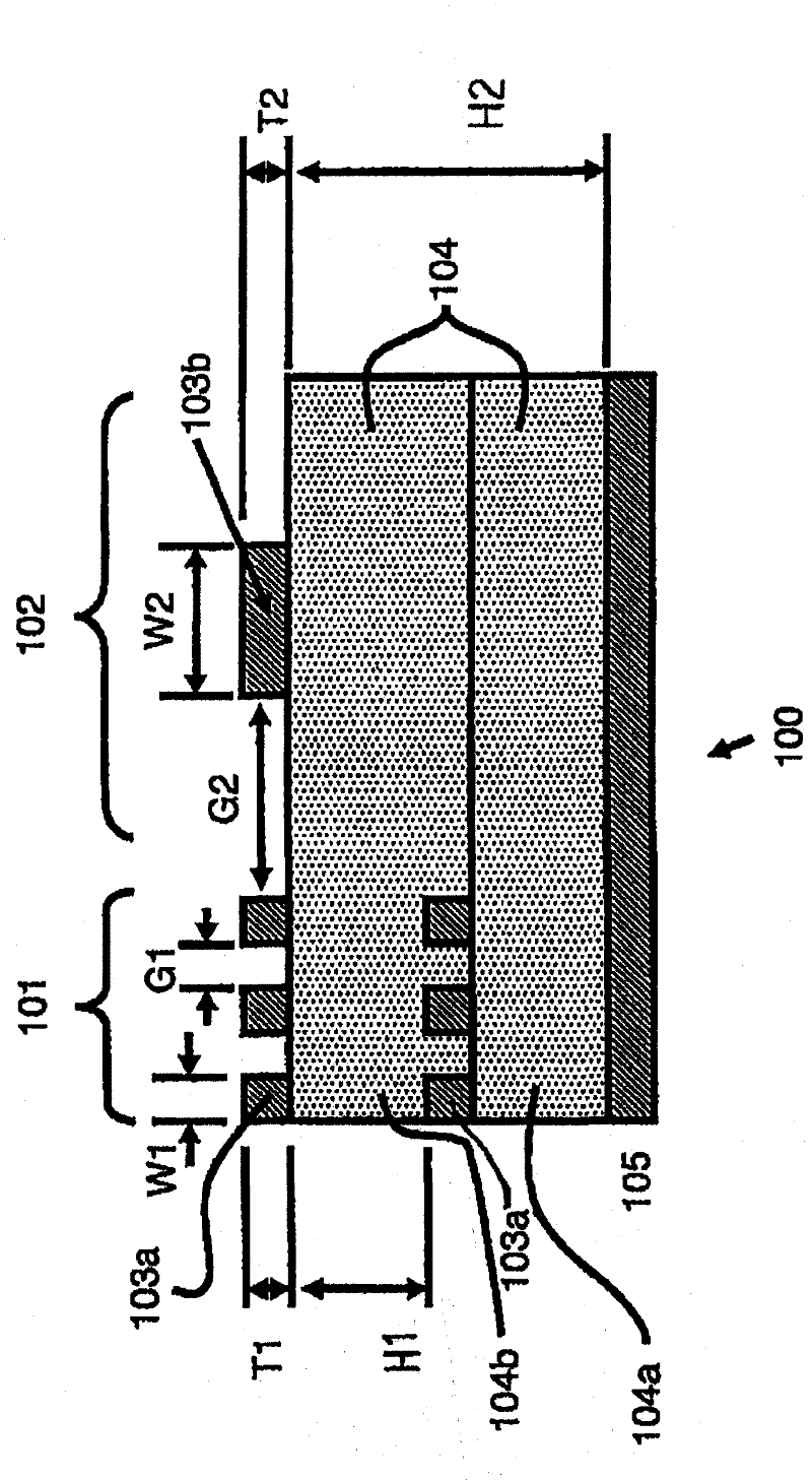
[0044] Such as figure 1 As shown, the multilayer wiring board 100 as the circuit board according to the first embodiment of the present invention has a first wiring region (multilayer wiring region) 101 and a second wiring region (multilayer wiring region) 102 . In the first wiring region (multilayer wiring region) 101, plate-like or film-like insulating layers 104a, 104b and wiring 103a are stacked on each other. The second wiring region (multilayer wiring region) 102 has wiring 103b on an insulating layer 104 having twice the thickness H1 of the insulating layer per one layer of the first wiring region 101. above the insulating layer thickness H2. The wiring width W2 of the wiring 103 b is set to be twice or more than the wiring width W1 of the wiring 103 a of the first wiring region 101 . 105 is a conductive film.

[0045] The multilayer wiring substrate 100 of the first ...

no. 2 approach

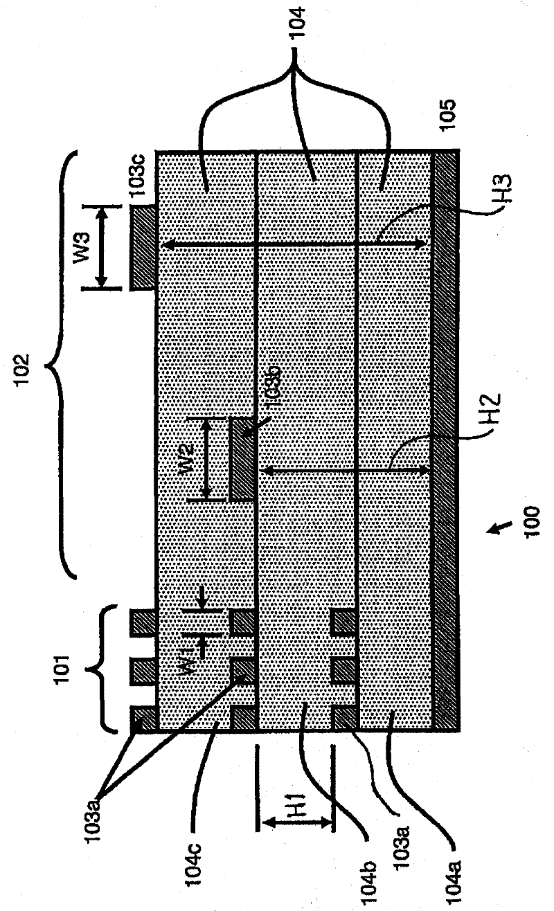
[0057] Below, refer to image 3 A second embodiment will be described.

[0058] Such as image 3 As shown, in the second embodiment, in figure 1 The insulating layer 104c is formed on the uppermost wirings 103a and 103b, and the wiring 103a is formed in the first wiring region 101 on the insulating layer 104c, but the wiring 103b is not formed in the second wiring region 102. The wiring 103c is formed in the second part of the first part. In the second portion of the second wiring region 102, no wiring layer is formed on the insulating layer below the uppermost wiring 103c, and the thickness H3 of the insulating layer becomes more than three times the thickness H1 of the insulating layer. In addition, the width W3 of the wiring 103c is also preferably larger than the width W2 of the wiring 103b of the first portion. In the second embodiment, the second wiring region (multilayer wiring region) 102 has an insulating layer thickness H1 per one layer of the first wiring region...

no. 3 approach

[0062] refer to Figure 4 , to describe the third embodiment.

[0063] With the third embodiment, it is formed so that in the boundary region between the first wiring region 101 and the second wiring region 102, a via hole (via hole), that is, a hole penetrating the insulating layer in the longitudinal direction, is provided, and the conductive The structure is the same as that of the first embodiment except for filling the hole with a conductive body and connecting the wiring 106 to the ground electrode 105 via the conductive body. By arranging the via conductor connected to the ground electrode 105 and the wiring 106, electrical coupling between the signal of the wiring in the first wiring region 101 and the signal of the wiring in the second wiring region 102 can be suppressed, Noise to signals transmitted in the second wiring region 102 can be suppressed.

[0064] Although in Figure 4 Although the wiring 106 is connected to the conductive film 105 as the ground electro...


PUM


Abstract

A multilayer wiring board (100) has a first wiring region (101) wherein a wiring (103a) and insulating layers (104a, 104b) are alternately laminated; and a second wiring region (102) wherein a thickness (H2) of an insulating layer (104) is double a thickness (H1) of an insulating layer of the first wiring region (101) or more, and a width (W2) of a wiring (103b) is double a wiring width (W1) or more. The first wiring region (101) and the second wiring region (102) are integrally formed on the same substrate.

Description

technical field [0001] The present invention relates to a multilayer wiring board including a substrate for mounting semiconductor elements such as LSIs and ICs, and particularly relates to a semiconductor element mounting substrate and a multilayer wiring board capable of reducing electrical signal loss in high-frequency applications. Background technique [0002] A multilayer wiring board constitutes a semiconductor device by mounting a semiconductor element and housing it together with the semiconductor element in the same package, or by mounting a plurality of electronic components (semiconductor device and other active body components, capacitors, and resistors) It is widely used to configure electronic devices such as information equipment, communication equipment, and display devices (eg, passive body parts such as components) (for example, refer to Patent Document 1). With the high-speed transmission and miniaturization of these semiconductor devices and information ...

Claims


Application Information

Patent Timeline
Patent Type & Authority Applications(China)
IPC IPC(8): H01L23/12H01P3/08H05K3/46
CPCH01L23/66H01L2223/6616H01L2223/6627H01L2223/6688H01L2924/19032H01L2924/3011H05K1/0218H05K1/025H05K1/0265H05K3/4652H05K2201/0191H05K2201/0352H05K2201/0715H05K2201/096H05K2201/09618H05K2201/09727H05K2201/09972H01L2924/0002H01L2924/00
Inventor 大见忠弘须川成利今井纮寺本章伸
Owner TOHOKU UNIV
Why Eureka
Try Eureka