Unit structure of multi-time programmable (MTP) device

A cell structure and device technology, applied in the NVM field, can solve the problems of limiting the maximum value of the erase voltage, low turn-on voltage of the parasitic MOS transistor 40, and low doping concentration, etc.

Active Publication Date: 2011-05-18
SHANGHAI HUAHONG GRACE SEMICON MFG CORP
View PDF3 Cites 4 Cited by
  • Summary
  • Abstract
  • Description
  • Claims
  • Application Information

AI Technical Summary

Problems solved by technology

Its gate oxide layer is a field region, and its thickness cannot be changed; its channel region, that is, the doping concentration of p-type impurities in the p-type substrate 41 is very low, so that the turn-on voltage of the parasitic MOS transistor 40 is also very low
This greatly limits the maximum value of the erasing voltage. The above-mentioned patent limits the erasing voltage below 7V, which is inseparable from the fear that the parasitic MOS transistor 40 will be turned on and the entire MTP device will fail.

Method used


Image

  • Unit structure of multi-time programmable (MTP) device
  • Unit structure of multi-time programmable (MTP) device
  • Unit structure of multi-time programmable (MTP) device

Examples


Embodiment Construction

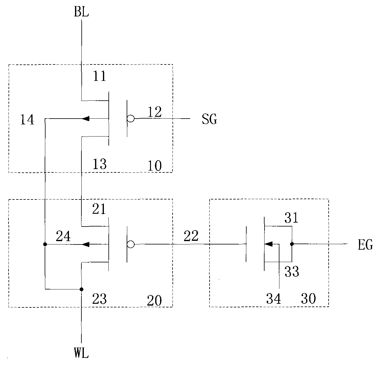
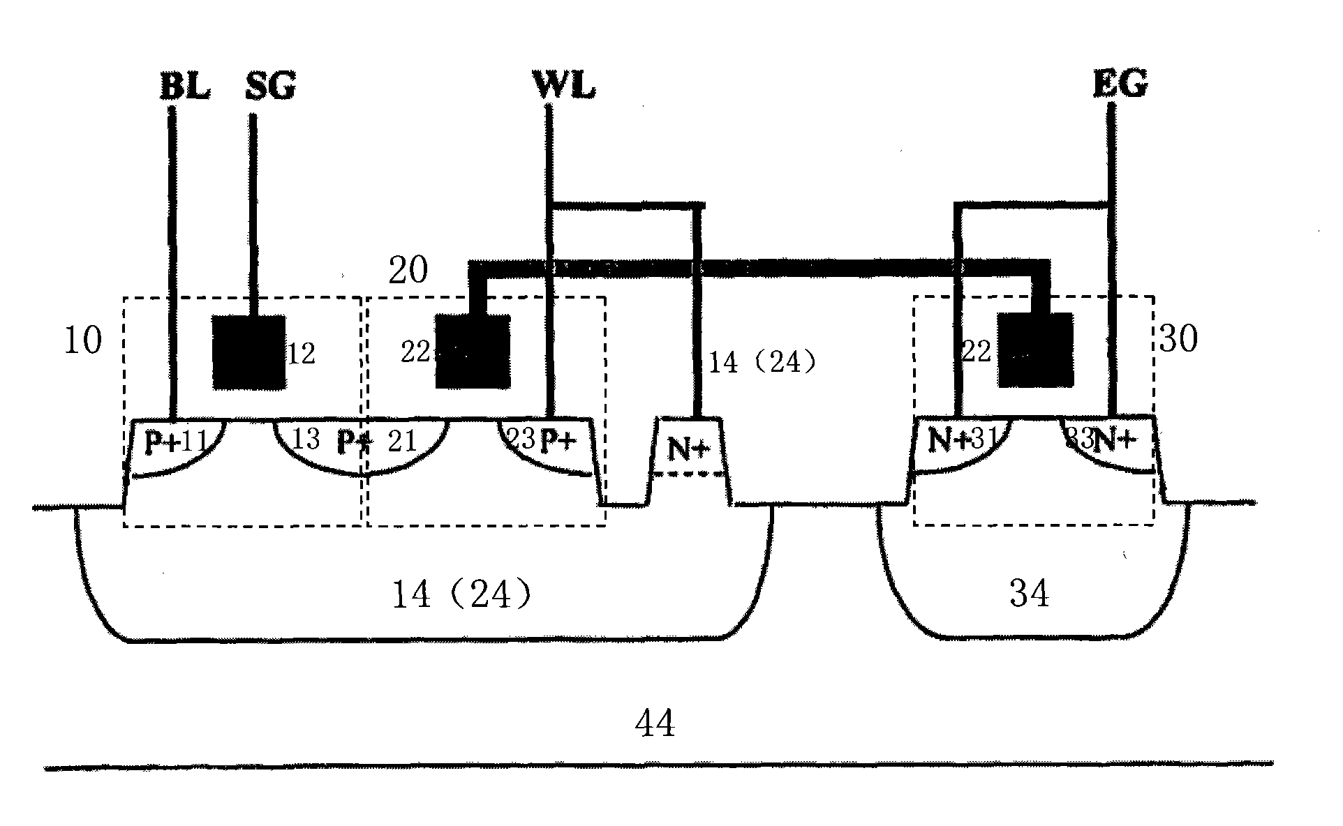
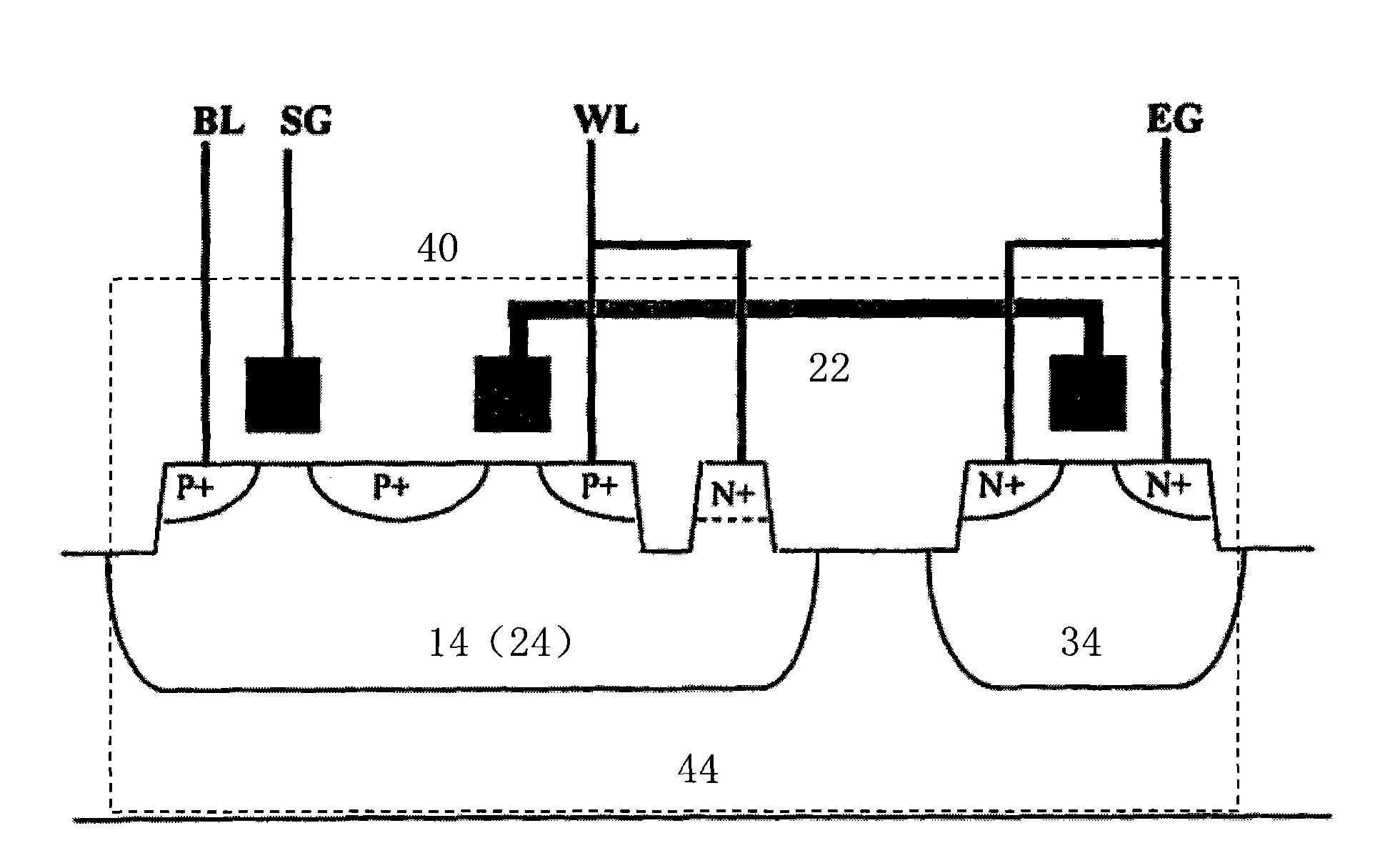
[0031] see Figure 4 The unit structure of the MTP device of the present invention includes a selection transistor 10 (PMOS), a programming transistor 20 (PMOS) and an erasing transistor 30 (PMOS), which are respectively located in n well 14, n well 24, and n well 34. The source 11 of the selection transistor 10 is connected to the n-well 14 and the n-well 24 and serves as the programming terminal WL. The gate 12 of the selection transistor 10 serves as the selection terminal SG. The drain 13 of the selection transistor 10 is connected to the source 21 of the programming transistor 20 . The gate of the programming transistor 20 and the gate of the erasing transistor 30 are the same polysilicon floating gate 22 . The drain 23 of the programming transistor 20 serves as the drain terminal BL. The source 31 , the drain 33 and the n-well 34 of the erasing transistor 30 are connected to each other and serve as an erasing terminal EG.

[0032] As described in the background art, ...


PUM


Abstract

The invention discloses a unit structure of a multi-time programmable (MTP) device. In the unit structure of the MTP device, an n well (24) is transversely isolated from an n well (34) through a p-type substrate (41) and a p well (42), and the p-type substrate (41) transversely contacts with the n well (34), so that larger breakdown voltage can be provided and an erase voltage is increased. The p well (42) is arranged between the n well (24) and the n well (34) and does not directly contact with the n well (34), so that the dosage concentration of p type impurities in a channel region of a parasitic metal oxide semiconductor (MOS) transistor is improved, a start voltage of the MOS transistor (40) is increased and the erase voltage is increased. According to the two factors, the maximum value of the erase voltage, which the unit structure of the MTP device can apply, is increased, so that higher erase speed and better erase effect can be achieved.

Description

technical field [0001] The present invention relates to an NVM (Non Volatile Memory, non-volatile memory), in particular to an MTP (Multi-Time Programmable, multi-programmable) NVM device. Background technique [0002] Chinese invention patent application publication specification CN101373634A (disclosure date: February 25, 2009) discloses a MTP device unit structure, which is composed of a selection transistor, a programming transistor and an erasing transistor. Both the selection transistor and the programming transistor are PMOS, and the erasing transistor can be either NMOS or PMOS. [0003] When the erasing transistor is PMOS, the unit structure of the MTP device is as follows figure 1 As shown, it includes a selection transistor 10 , a programming transistor 20 and an erasing transistor 30 , which are respectively located in the n well 14 , n well 24 and n well 34 . The source 11 of the selection transistor 10 is used as the drain BL, the gate 12 of the selection tra...

Claims


Application Information

Patent Timeline
Patent Type & Authority Applications(China)
IPC IPC(8): G11C16/04H01L27/115
Inventor 徐向明胡晓明
Owner SHANGHAI HUAHONG GRACE SEMICON MFG CORP
Why Eureka
Try Eureka