Unit structure of multi-time programmable (MTP) device
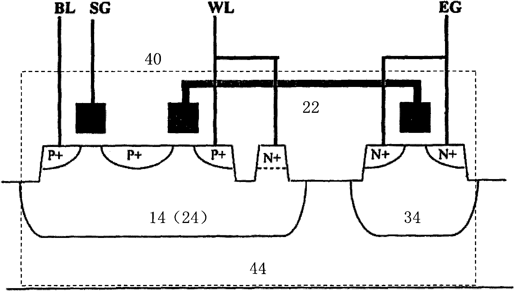
A cell structure and device technology, applied in the NVM field, can solve the problems of limiting the maximum value of the erase voltage, low turn-on voltage of the parasitic MOS transistor 40, and low doping concentration, etc.
- Summary
- Abstract
- Description
- Claims
- Application Information
AI Technical Summary
Problems solved by technology
Method used
Image
Examples
Embodiment Construction
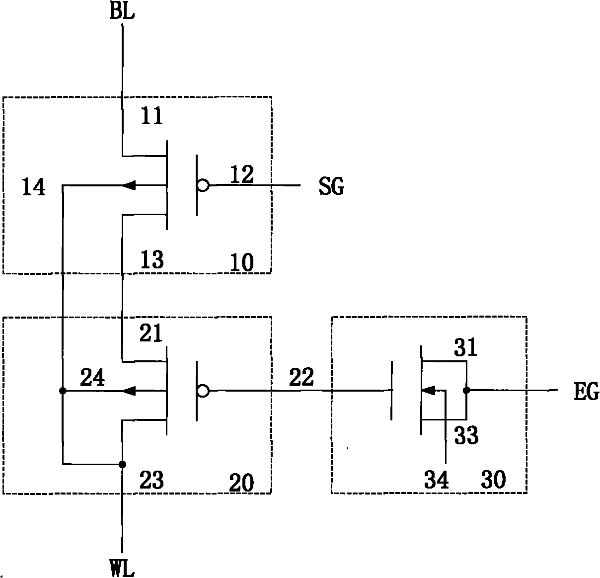
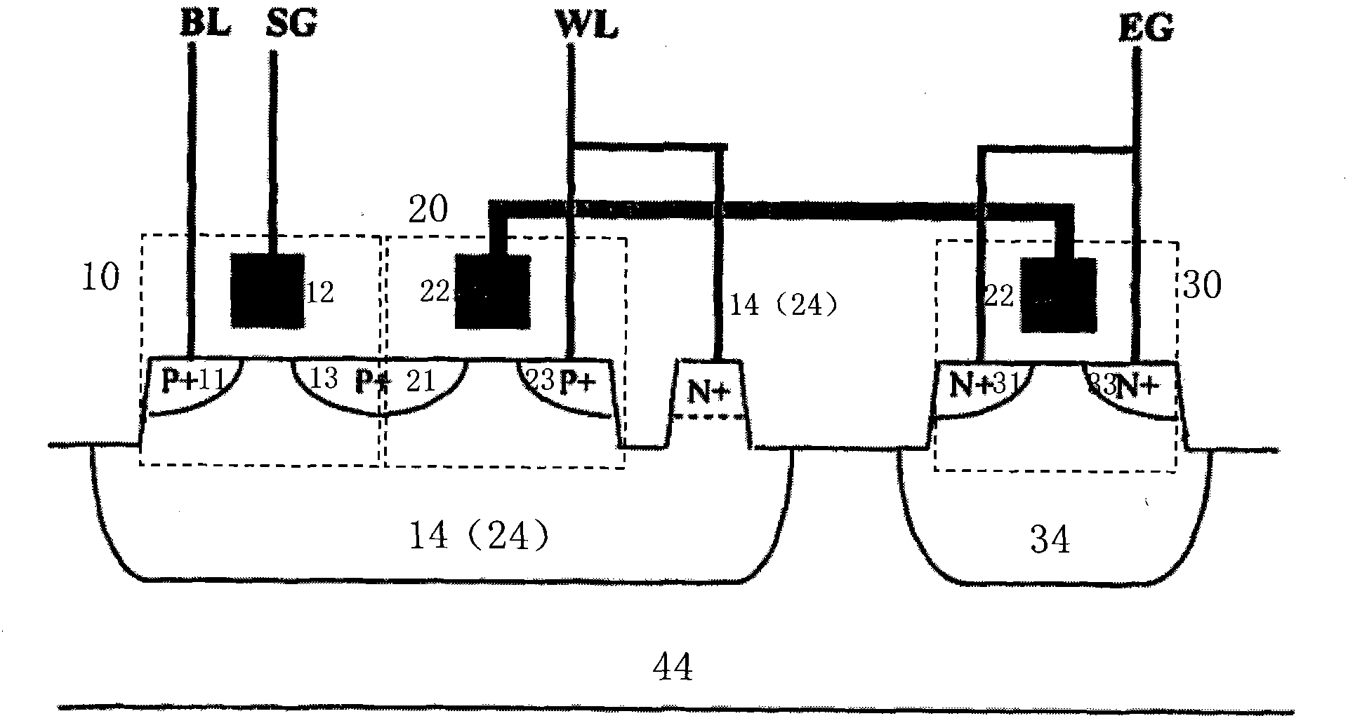
[0031] see Figure 4 The unit structure of the MTP device of the present invention includes a selection transistor 10 (PMOS), a programming transistor 20 (PMOS) and an erasing transistor 30 (PMOS), which are respectively located in the n well 14, n well 24, and n well 34. The source 11 of the selection transistor 10 is connected to the n-well 14 and the n-well 24 and serves as the programming terminal WL. The gate 12 of the selection transistor 10 serves as the selection terminal SG. The drain 13 of the selection transistor 10 is connected to the source 21 of the programming transistor 20 . The gate of the programming transistor 20 and the gate of the erasing transistor 30 are the same polysilicon floating gate 22 . The drain 23 of the programming transistor 20 serves as the drain terminal BL. The source 31 , the drain 33 and the n-well 34 of the erasing transistor 30 are connected to each other and serve as an erasing terminal EG.
[0032] As described in the background a...
PUM
 Abstract
Description
Claims
Application Information
 - R&D
- Intellectual Property
- Life Sciences
- Materials
- Tech Scout
- Unparalleled Data Quality
- Higher Quality Content
- 60% Fewer Hallucinations
Browse by: Latest US Patents, China's latest patents, Technical Efficacy Thesaurus, Application Domain, Technology Topic, Popular Technical Reports.
© 2025 PatSnap. All rights reserved.Legal|Privacy policy|Modern Slavery Act Transparency Statement|Sitemap|About US| Contact US: help@patsnap.com


