Production method of high-density laminated printed circuit board of high-frequency material

A technology for printed circuit boards and high-frequency materials, applied in the direction of multi-layer circuit manufacturing, etc., can solve the problems of high cost, removal of high-frequency materials, and high safety hazards of sulfuric acid, so as to enhance the bonding force between layers and improve reliability. , the effect of high safety

Inactive Publication Date: 2011-05-18
GUANGZHOU FASTPRINT CIRCUIT TECH
View PDF3 Cites 27 Cited by
  • Summary
  • Abstract
  • Description
  • Claims
  • Application Information

AI Technical Summary

Problems solved by technology

The production process of this kind of board is complicated, and many processes are difficult to manufacture. In addition to the common problems of high-density laminates: drilling, lamination, electroplating, etching and other processes, there is another thorny problem, which is this kind of high-frequency material board. Blind Hole Removal
However, for high-density laminated printed circuit boards using high-frequency material prepregs, the glue removal process before copper sinking cannot remove the high-frequency material overflowing from blind holes after lamination, which will directly lead to poor copper sinking and scrap the board
In order to solve this kind of problem, the following methods are often used at present: ① Soak in pure sulfuric acid directly to remove glue residue. At the same time, sulfuric acid has a great safety hazard in the operation process; ② Use a ceramic grinding machine to grind the plate to remove glue residue. Because the plate surface is uneven, the pressure of the ceramic grinding plate is difficult to control, and the base is often exposed due to the grinding plate The material is scrapped; and the ceramic plate grinding machine is expensive and the cost is high

Method used


Image

  • Production method of high-density laminated printed circuit board of high-frequency material
  • Production method of high-density laminated printed circuit board of high-frequency material
  • Production method of high-density laminated printed circuit board of high-frequency material

Examples


Embodiment Construction

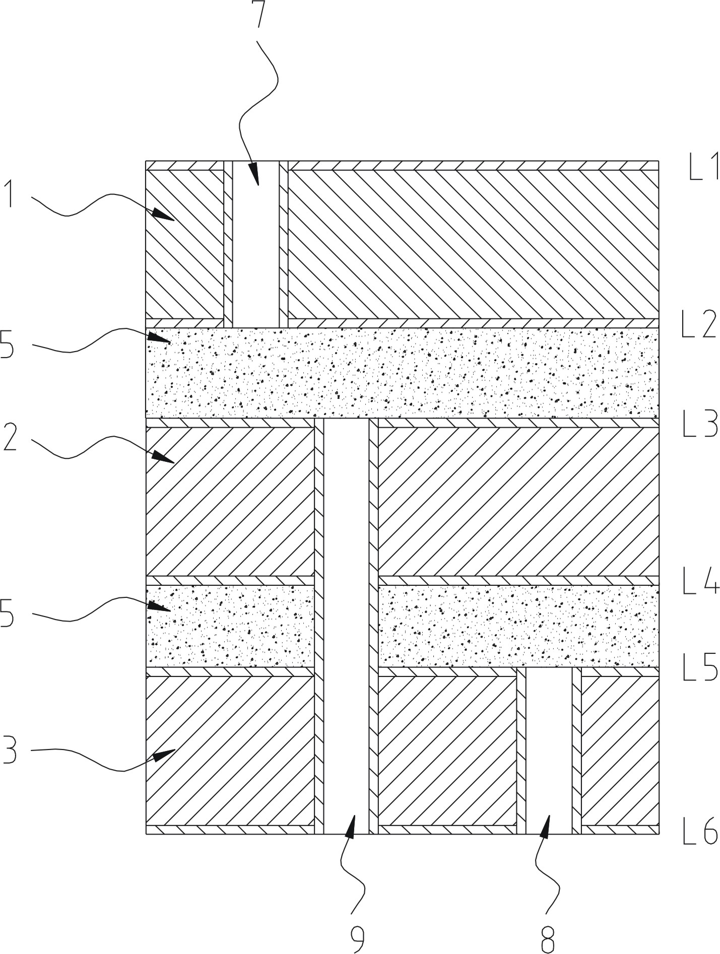
[0019] figure 1 Shown is a schematic structural diagram of a high-density laminated board with 6 layers of high-frequency materials. This board is composed of three high-frequency board sub-boards 1, 2, and 3 and several high-frequency prepregs 5, 6. Among them, There are three types of blind holes in the board design, one is blind holes 7 on layers L1-L2, one is blind holes 9 on layers L3-L6, and the other is blind holes 8 on layers L5-L6. Its processing flow is as follows.

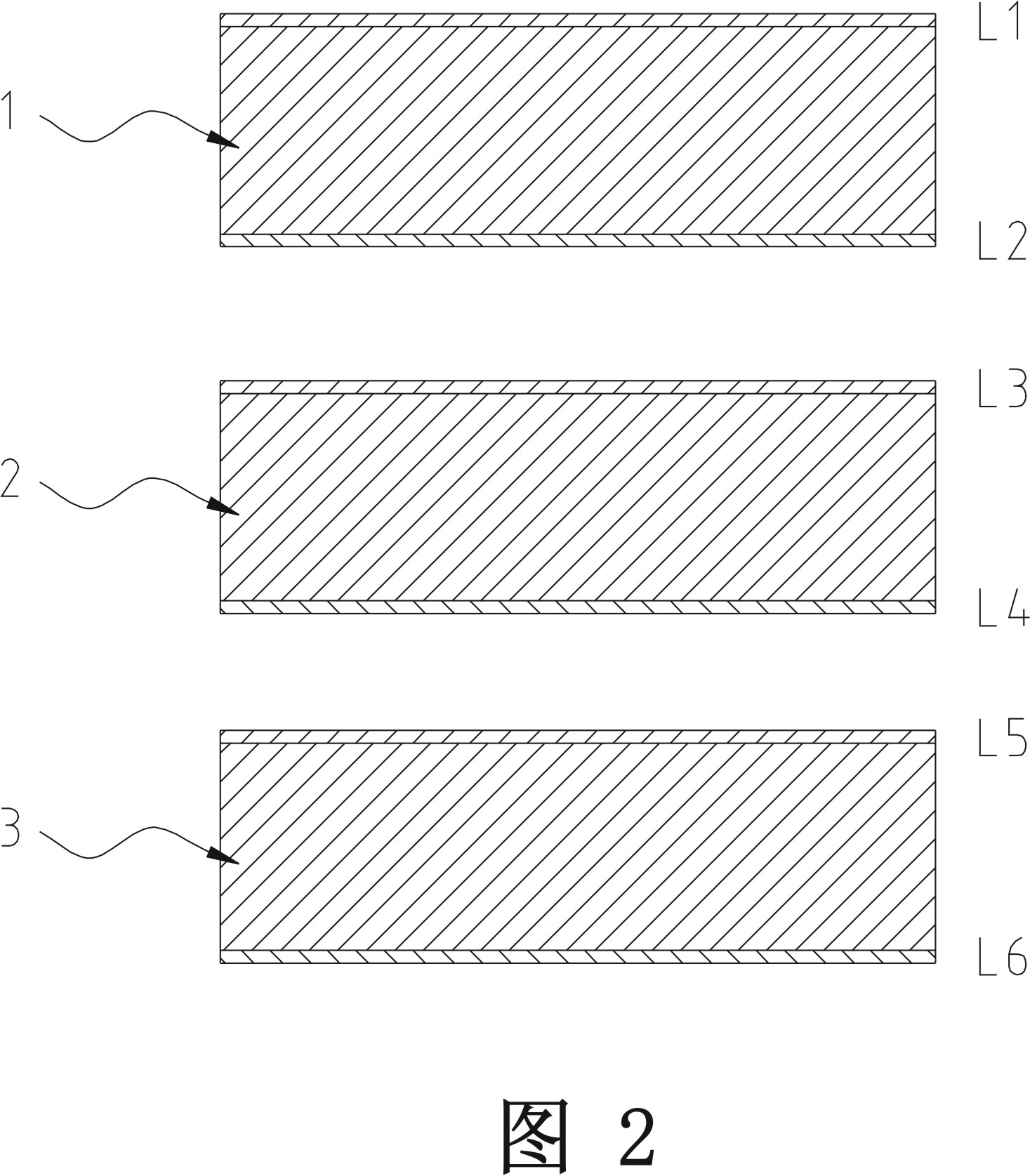
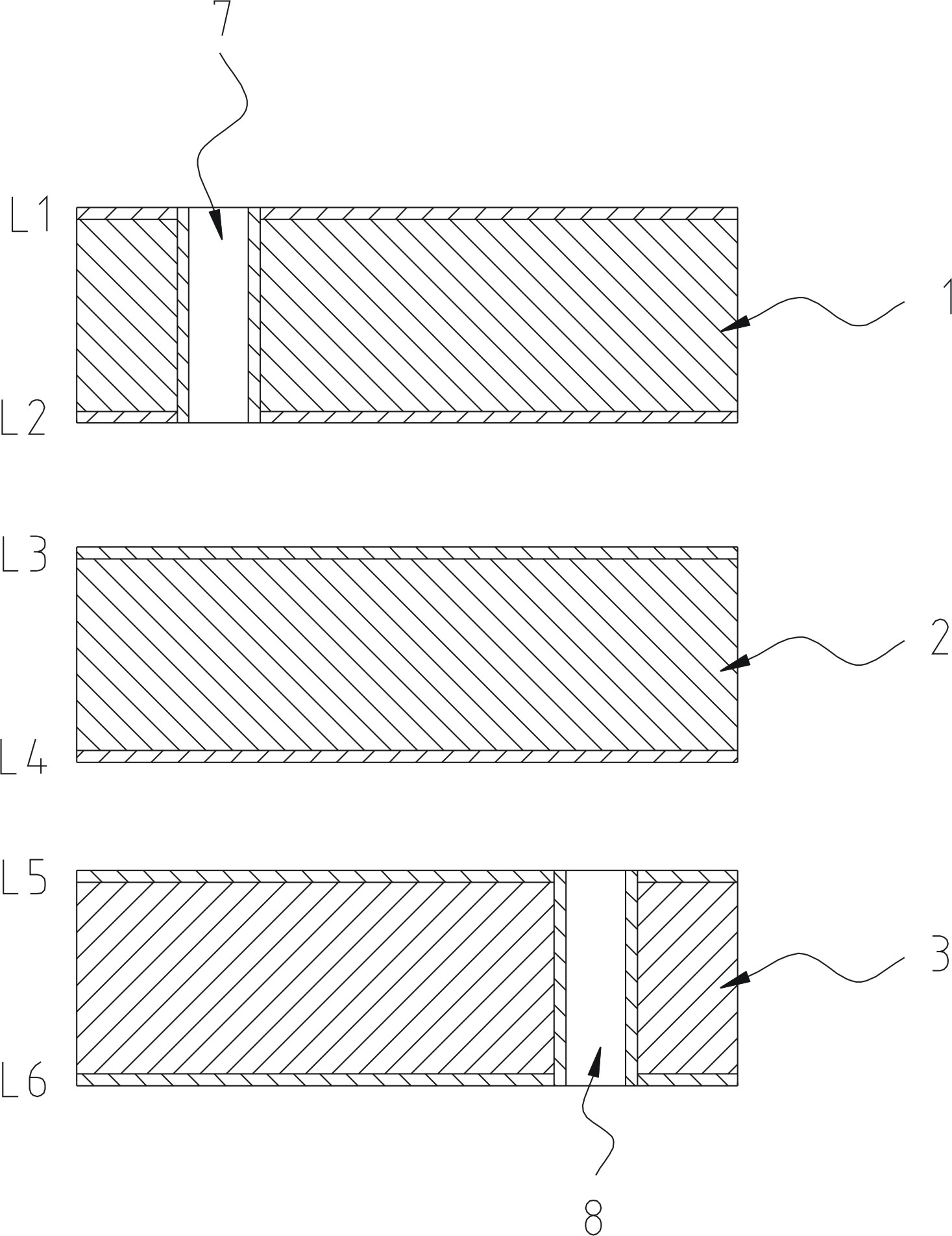
[0020] (1) Complete the production of sub-board 1, sub-board 2 and sub-board 3 respectively: see figure 2 , 3 The sub-board 1 completes the production of the blind hole 7 and the L2 layer circuit; the sub-board 2 completes the production of the L4 layer circuit; the sub-board 3 completes the production of the blind via 8 and the L5 layer circuit.

[0021] (2) Silk screen solder mask: see Figure 4 Firstly, the sub-board 3 is ground through the solder mask pretreatment line to clean the board surface...


PUM


Abstract

The invention discloses a production method of a high-density laminated printed circuit board of a high-frequency material. The production method comprises the following steps of: (1) drilling: drilling blind holes for interlaminar electrical connection on a layer or a plurality of layers of daughter boards; (2) screen printing solder resist: coating solder resist printing ink on the surface of outer copper foil of the layer or the plurality of layers of daughter boards with the blind holes, ensuring that the blind holes are filled with the solder resist printing ink, and exposing and developing to solidify the solder resist printing ink; (3) laminating: laminating the layer or the plurality of layers of daughter boards having the solder resist printing ink with other daughter boards into a whole by high-frequency prepregs; and (4) taking off the solder resist printing ink. The production method provided by the invention can commendably solve the problem that glue is difficult to remove when the high-density laminated printed circuit board of the high-frequency material is laminated and has the advantages of simpleness and safety of operation and low cost. In addition, the production method can play a role of glue resistance so that resin can not overflow to the board surface and is kept on interlamination, thereby effectively strengthening interlaminar bonding force and improving reliability of a product.

Description

technical field [0001] The invention relates to a method for manufacturing a printed circuit board, in particular to a method for producing a high-density laminated printed circuit board of high-frequency materials. Background technique [0002] At present, there are two main development trends of electronic products, one is high density and high integration, and the other is high speed and high frequency. For PCB, on the one hand, in order to achieve high-density interconnection, more and more multi-level blind buried holes are used. On the other hand, in order to achieve high frequency, more and more high-frequency materials are used for production. As the demand for electronic products requiring both high density and high frequency increases, the production volume of high-density build-up printed circuit boards using high-frequency materials is increasing. The production process of this kind of board is complicated, and many processes are difficult to manufacture. In add...

Claims


Application Information

Patent Timeline
Patent Type & Authority Applications(China)
IPC IPC(8): H05K3/46
Inventor 乔书晓田玲刘湘龙
Owner GUANGZHOU FASTPRINT CIRCUIT TECH
Why Eureka
Try Eureka