Wire connecting method for line repair

A wiring and circuit technology, applied in the field of semiconductor circuit repair, can solve problems such as accidental short circuit, poor contact, platinum discontinuity, etc., and achieve the effect of improving current function debugging, improving success rate and saving costs.

Active Publication Date: 2011-05-25
SHANGHAI HUAHONG GRACE SEMICON MFG CORP
View PDF6 Cites 7 Cited by
  • Summary
  • Abstract
  • Description
  • Claims
  • Application Information

AI Technical Summary

Problems solved by technology

[0003] 1. When the metal line to be repaired is more than 2 layers of metal layer and insulating layer (or more than 1 micron in height) from the surface of the silicon chip, due to the large drop, when the platinum is plated, there will be poor contact, resulting in a large impedance Or not connected at all, the performance is (1) When the window is small, the platinum deposition process is similar to the metal sputtering filling in the semiconductor process. The larger the aspect ratio, the larger the gap in the middle of the hole, resulting in a large resistance, and even the middle The gap directly cuts off the upper and lower connections of platinum. (2) When the window is large, the interconnection can be completed by lengthening the accumulation time, but the large window will easily lead to the exposure of non-target metal wires, and it is easy to form an accidental short circuit; figure 1 is a side view of question 1
[0004] 2. When the window is controlled to be larger, and when the metal lines on the same layer are relatively dense, the large window will expose other non-target metal lines, and accidental short circuits are likely to occur when interconnecting
figure 2 Shown is a side view of problem 2, the larger the aspect ratio, the larger the gap, so that the platinum fill is discontinuous, causing high impedance or open circuit

Method used


Image

  • Wire connecting method for line repair
  • Wire connecting method for line repair
  • Wire connecting method for line repair

Examples


Embodiment Construction

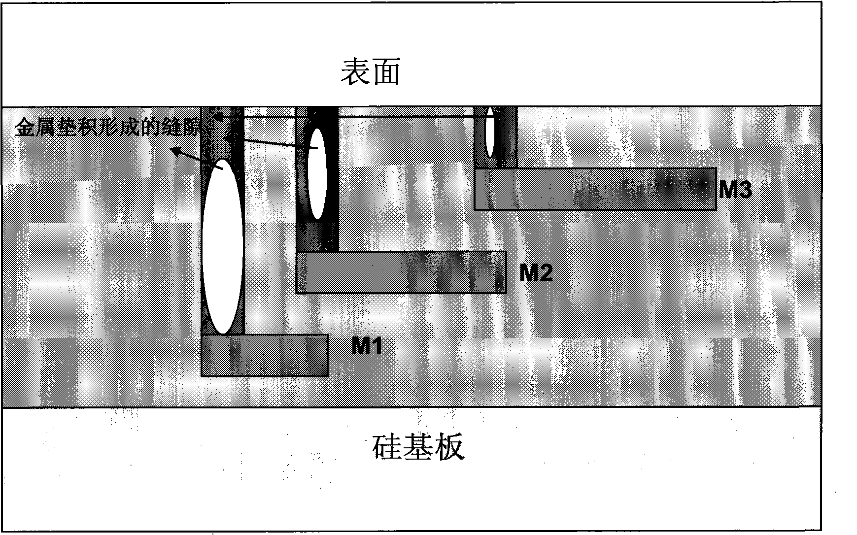
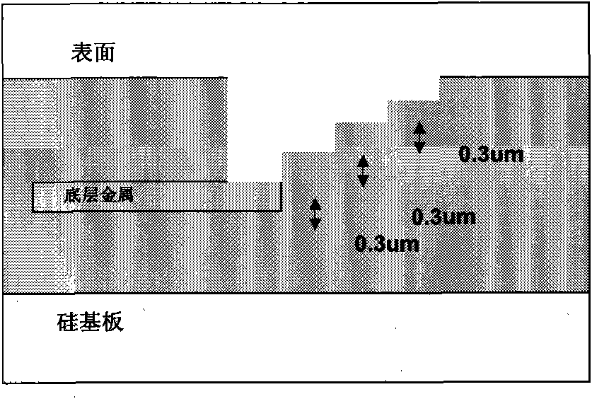
[0028] Focused Ion Beam Electron Microscope FIB (Focused Ion Beam): It uses the focused gallium positive ion beam as the incident particle (or primary ion) to hit the surface of the sample, and collects secondary electrons for imaging. Due to the large atomic weight of gallium ions, it accelerates The rear kinetic energy is large, so it has a good sputtering etching function, and with a suitable gas system, auxiliary functions including selective etching and depositing specific materials can be realized. The gas system it is often equipped with is Pt-Dep (platinum metal deposition system), IEE (selective enhanced etching), I-dep (insulation film deposition), etc.; when working, the gas is sprayed on the surface of the sample, and the ion beam bombards When FIB sets the pattern, it not only directly etches the sample surface, but also impacts some gas atoms on the sample surface; by adjusting appropriate parameters, a layer of platinum metal film can be deposited with Pt-dep, an...


PUM


Abstract

The invention discloses a wire connecting method for line repair. The method comprises the following steps of: 1, forming a small window above an insulating film at a specified metal wire position to be repaired; 2, fixing the wide edge of one side of the etched window, elongating the long edge, keeping the size of the wide edge unchangeable, and etching with depth of 0.1 to 0.5 micron; if a metal wire is exposed at the determined position of the etched window, stopping etching, otherwise, fixing the wide edge again, elongating the long edge and etching with depth of 0.1 to 0.5 micron; circulating the step till the metal wire is exposed; and 3, plating a platinum wire with a length equal to the wire connecting distance along a step from the position of the exposed metal wire so as to realize wire connection. The method improves the velocity and success rate of the line repair, saves certain expensive materials, and greatly quickens the progress of chip problem debugging.

Description

technical field [0001] The invention relates to a semiconductor circuit repair method, in particular to a circuit repair technology used in semiconductor chip debugging and failure analysis. Background technique [0002] At present, the direct etching single window connection method of the focused particle beam electron microscope FIB (Focused Ion Beam) commonly used in the field of semiconductor circuit repair has the following problems: [0003] 1. When the metal line to be repaired is more than 2 layers of metal layer and insulating layer (or more than 1 micron in height) from the surface of the silicon chip, due to the large drop, when the platinum is plated, there will be poor contact, resulting in a large impedance Or not connected at all, the performance is (1) When the window is small, the platinum deposition process is similar to the metal sputtering filling in the semiconductor process. The larger the aspect ratio, the larger the gap in the middle of the hole, resu...

Claims


Application Information

Patent Timeline
Patent Type & Authority Applications(China)
IPC IPC(8): H01L21/768
Inventor 赖华平
Owner SHANGHAI HUAHONG GRACE SEMICON MFG CORP
Why Eureka
Try Eureka