Manufacturing method of display panel and display device

A technology for display panels and manufacturing methods, applied in optics, instruments, nonlinear optics, etc., can solve the problems of easy coating with pores, unevenness, and difficult control of the quality of alignment substrates, etc., to ensure quality and yield , Improve the effect of quality and yield

Inactive Publication Date: 2011-06-01
TCL CHINA STAR OPTOELECTRONICS TECH CO LTD
View PDF6 Cites 17 Cited by
  • Summary
  • Abstract
  • Description
  • Claims
  • Application Information

AI Technical Summary

Problems solved by technology

[0004] However, the coating process (such as inkjet printing) of this alignment substrate (polyimide) is prone to defects such as pin holes or uneven coating (mura)
Furthermore, the polyimide after coating needs to be cured, and the polyimide is easy to absorb moisture
Therefore, the quality of the existing alignment substrate is not easy to control, thus affecting the process yield of the display panel

Method used


Image

  • Manufacturing method of display panel and display device
  • Manufacturing method of display panel and display device
  • Manufacturing method of display panel and display device

Examples


Embodiment Construction

[0041] The following descriptions of the various embodiments refer to the accompanying drawings to illustrate specific embodiments in which the present invention can be practiced. The directional terms mentioned in the present invention, such as "up", "down", "front", "back", "left", "right", "inside", "outside", "side", etc., are for reference only The orientation of the attached schema. Therefore, the directional terms used are used to illustrate and understand the present invention, but not to limit the present invention.

[0042] In the figures, structurally similar units are denoted by the same reference numerals.

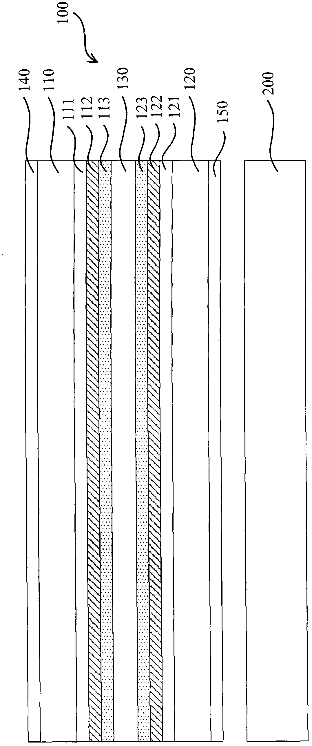
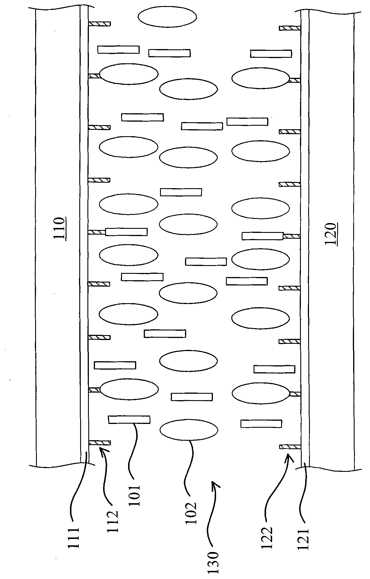
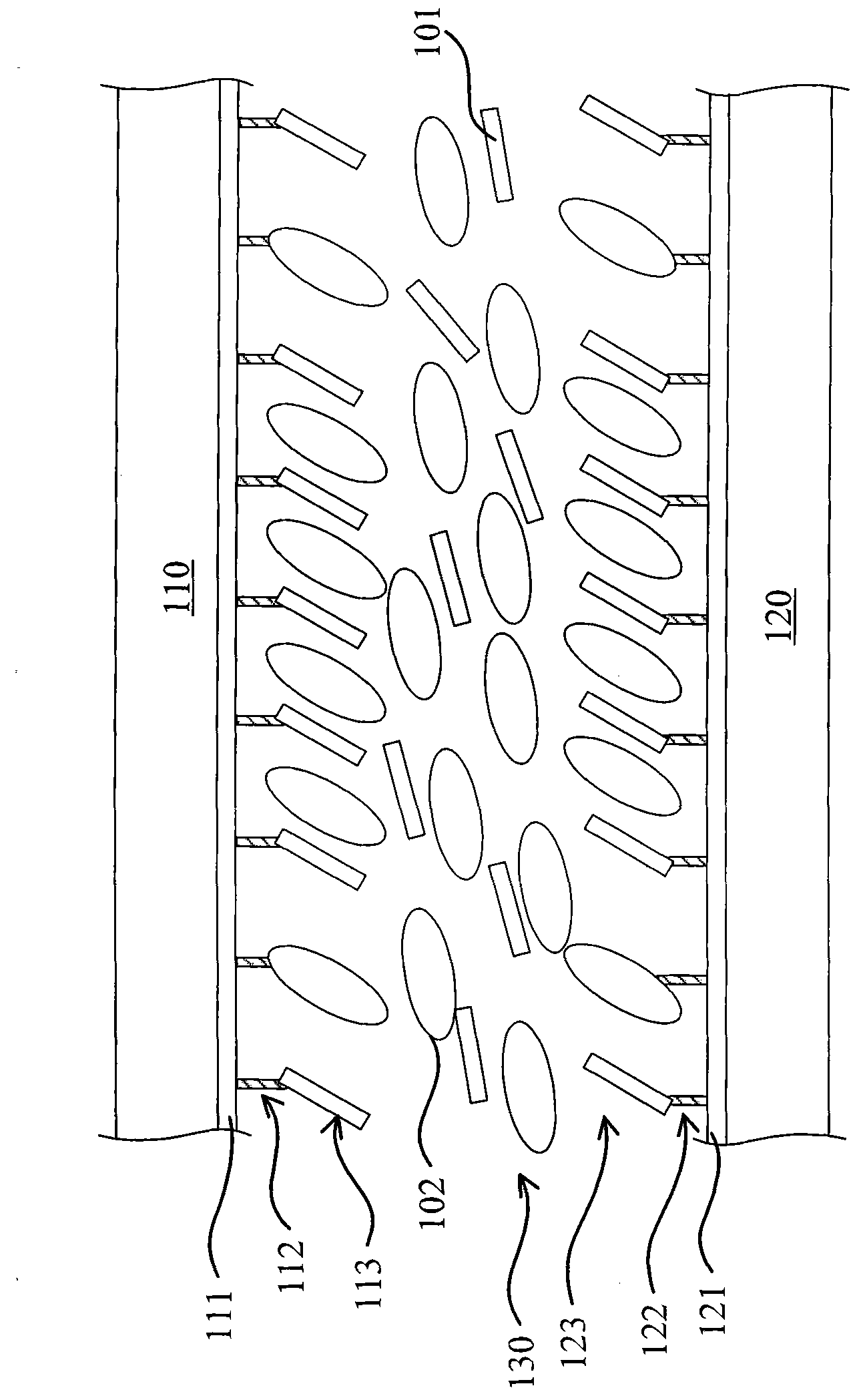
[0043] Please refer to figure 1 , which shows a schematic cross-sectional view of a display panel and a backlight module according to an embodiment of the present invention. The liquid crystal display device of this embodiment may include a liquid crystal display panel 100 and a backlight module 200 . The liquid crystal display panel 100 is disposed relati...


PUM


Abstract

The invention provides a manufacturing method of a display panel and a display device. The method comprises the following steps of: sputtering alignment layers on a substrate; forming a liquid crystal layer between the alignment layers to form a liquid crystal box; applying a voltage to the liquid crystal box; irradiating ultraviolet light on the liquid crystal box; and arranging the display panel on a backlight module. The quality of an alignment film of the display panel can be improved with the method.

Description

【Technical field】 [0001] The invention relates to the technical field of liquid crystal display, in particular to a method for manufacturing a display panel and a display device. 【Background technique】 [0002] Liquid Crystal Displays (LCDs) have been widely used in various electronic products. Most of the LCDs are backlight LCDs, which are composed of a liquid crystal display panel and a backlight module. A liquid crystal display panel is composed of two transparent substrates and a liquid crystal sealed between the substrates. In particular, a liquid crystal display panel with multi-domain alignment manufactured by a polymer-stabilized alignment (PSA) process can have a wide viewing angle, a high aperture ratio, and a high contrast And the advantages of simple manufacturing process. [0003] In the PSA process, the liquid crystal between the two transparent substrates can be doped with reactive monomer (reactive monomer), which is mixed with the liquid crystal molecules,...

Claims


Application Information

Patent Timeline
Patent Type & Authority Applications(China)
IPC IPC(8): G02F1/1333G02F1/1337
CPCG02F1/133734G02F1/1333G02F2001/13345G02F1/1334G02F1/13345
Inventor 贺成明李为钧廖炳杰
Owner TCL CHINA STAR OPTOELECTRONICS TECH CO LTD
Why Eureka
Try Eureka