

Electro-optic diode devices
A technology of diodes and devices, applied in the field of high-efficiency electro-optic diode devices
- Summary
- Abstract
- Description
- Claims
- Application Information
AI Technical Summary
Problems solved by technology
Method used
Image

Examples
Embodiment Construction
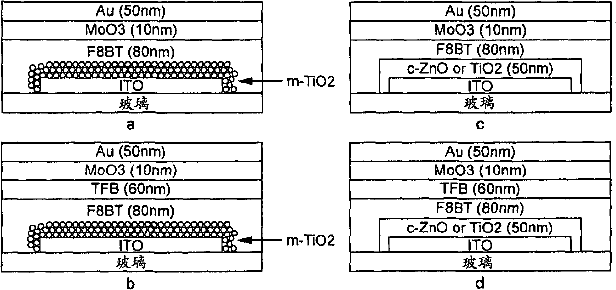
[0033] Light emitting devices to be described below use various metal oxides in mesoporous and compact forms for electron injection. It has been found that this results in high brightness COPLEDs. In one device form that has been found to be particularly effective, ZnO is used as the electron transport and injection material and MoO 3 Used as a hole injection material. In addition, the structure leaves room for the choice of component thickness and materials to enhance photonic effects.
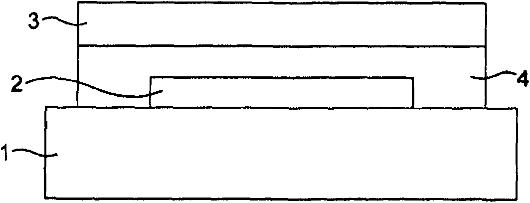
[0034] Device structure
[0035] A schematic basic form of the device described herein is shown in figure 1 middle. The device comprises a substrate 1 (eg glass) on which is deposited a cathode structure 2 for electron transport and injection, and an anode structure 3 for hole transport and injection. The light emitting structure 4 is sandwiched between the cathode and the anode. In the devices that have been studied, the cathode, anode and light-emitting structures take the form of lay...
PUM
| Property | Measurement | Unit |
|---|---|---|
| Length | aaaaa | aaaaa |
Abstract
Description
Claims
Application Information