Anti-single event effect static random access memory unit

An anti-single event effect, memory cell technology, applied in the field of static random access memory, can solve problems such as pulling down the voltage of the output terminal

Inactive Publication Date: 2011-06-15
INST OF SEMICONDUCTORS - CHINESE ACAD OF SCI
View PDF4 Cites 36 Cited by
  • Summary
  • Abstract
  • Description
  • Claims
  • Application Information

AI Technical Summary

Problems solved by technology

In an SRAM unit, if the closed NMOS transistor is in the open state, the voltage at the output terminal will be pulled down, causing the stored content to flip

Method used


Image

  • Anti-single event effect static random access memory unit
  • Anti-single event effect static random access memory unit
  • Anti-single event effect static random access memory unit

Examples


Embodiment Construction

[0024] In order to make the object, technical solution and advantages of the present invention clearer, the present invention will be described in further detail below in conjunction with specific embodiments and with reference to the accompanying drawings.

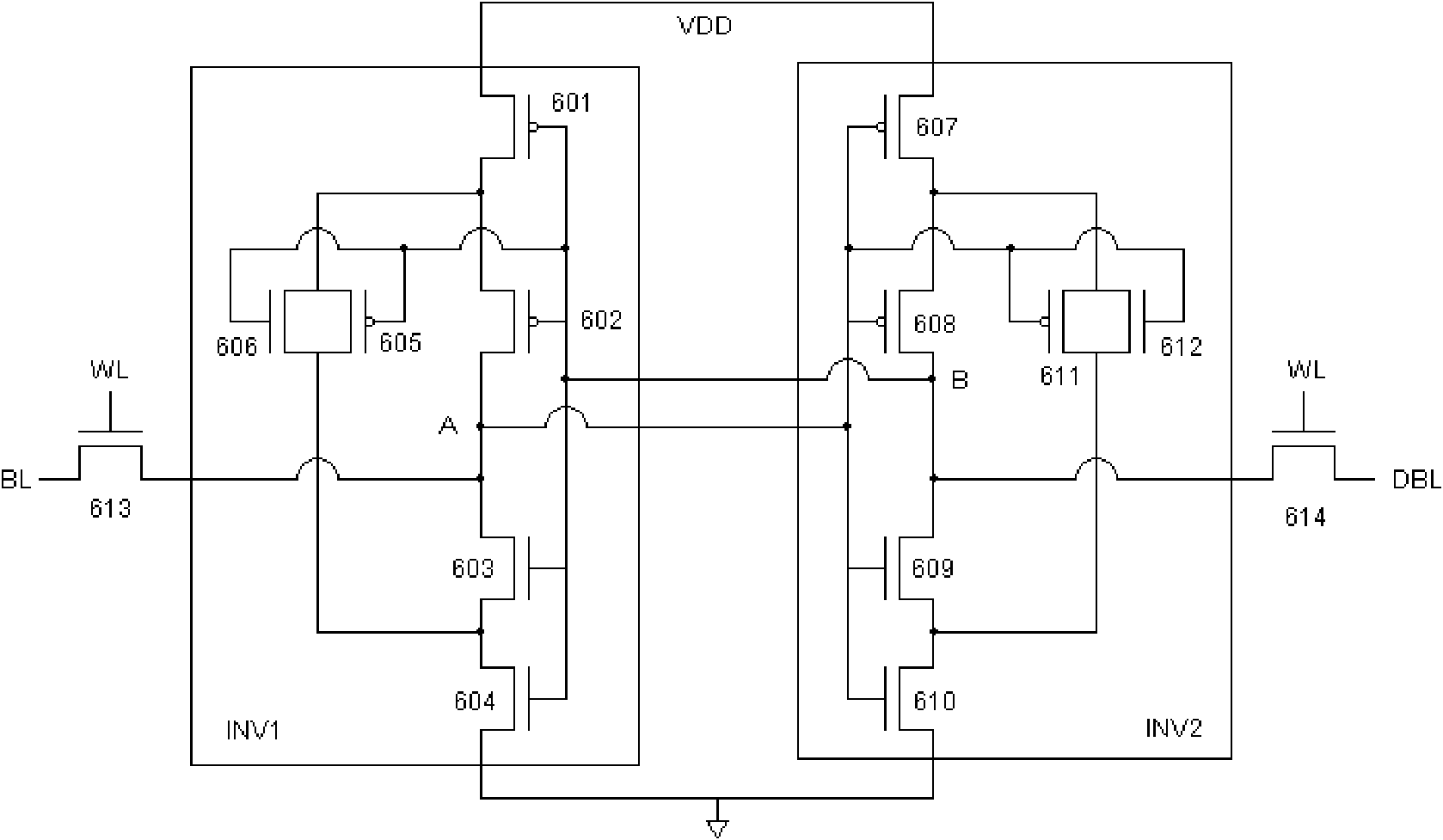
[0025] Such as figure 2 as shown, figure 2 It is the circuit diagram of the anti-single event flipping SRAM unit provided by the present invention, including the first inverter INV1, the second inverter INV2, the first NMOS transmission gate 613, and the second NMOS transmission gate 614, wherein: the first inverter The output terminal A of INV1 is connected to the first NMOS transmission gate 613, the output terminal B of the second inverter INV2 is connected to the second NMOS transmission gate 614, and the gate of the first NMOS transmission gate 613 and the gate of the second NMOS transmission gate 614 are connected to WL , the first NMOS transmission gate 613 corresponds to the unit output BL, the second NMOS tran...


PUM


Abstract

The invention discloses an anti-single event effect static random access memory unit, which can effectively improve the single event upset resistance of a static random access memory (SRAM) unit and remarkably increase an upset threshold of an SRAM. The SRAM unit is a 14-transistor memory unit, and comprises two access N-channel metal oxide semiconductor (NMOS) transistors and two phase inverters, wherein each phase inverter consists of six metal oxide semiconductor (MOS) transistors. Different from the phase inverters forming the most basic six-transistor unit, the inverter structure of the anti-single event effect SRAM unit regulates a level by the two NMOS transistors as drive transistors, two P-channel metal oxide semiconductor (PMOS) transistors as load transistors and a transmission gate consisting of the PMOS transistor and the NMOS transistor so as to realize the anti-single event upset of the memory unit. The SRAM unit has a relatively simpler structure, and is easy to realize in the designing of a radiation resistant SRAM chip.

Description

technical field [0001] The invention relates to the technical field of Static Random Access Memory (SRAM), and more particularly, relates to a CMOS SRAM unit with anti-single event upset effect. Background technique [0002] According to the data storage method, semiconductor memory is divided into dynamic random access memory (DRAM), non-volatile memory and static random access memory (SRAM). SRAM has established its unique advantage by being able to achieve fast operating speeds in a simple and low power consumption manner. Also, compared to DRAM, SRAM is relatively easy to design and manufacture because it does not need to periodically refresh the stored information. [0003] Typically, an SRAM cell consists of two drive transistors, two load devices, and two access transistors. According to the type of load device contained, SRAM itself can be divided into complete CMOSSRAM, high load resistance (High Load Resistor) SRAM and thin film transistor (Thin FilmTransistor) S...

Claims


Application Information

Patent Timeline
Patent Type & Authority Applications(China)
IPC IPC(8): G11C11/413
Inventor 李振涛乔宁
Owner INST OF SEMICONDUCTORS - CHINESE ACAD OF SCI
Why Eureka
Try Eureka