Method for manufacturing semiconductor device

A manufacturing method and semiconductor technology, applied in semiconductor/solid-state device manufacturing, electrical components, circuits, etc., can solve problems affecting junction depth, impurity concentration changes, device performance degradation, etc., to improve quality, avoid excessive losses, and benefit the process integrated effect

Inactive Publication Date: 2012-06-06
SEMICON MFG INT (SHANGHAI) CORP
View PDF0 Cites 0 Cited by
  • Summary
  • Abstract
  • Description
  • Claims
  • Application Information

AI Technical Summary

Problems solved by technology

The hydrogen atoms in the pad oxide layer will accelerate the diffusion of boron ions in the lightly doped source region and the lightly doped drain region to the pad oxide layer, resulting in significant impurity concentrations in the lightly doped source region and lightly doped drain region. changes, affecting junction depth and degrading device performance

Method used


Image

  • Method for manufacturing semiconductor device
  • Method for manufacturing semiconductor device
  • Method for manufacturing semiconductor device

Examples


Embodiment Construction

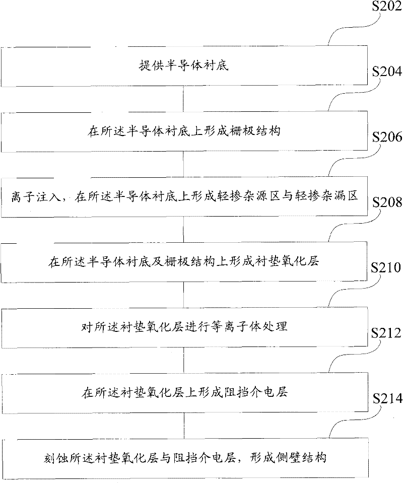
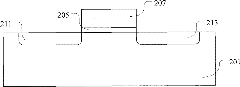
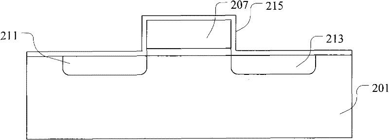
[0025] In the prior art, in the manufacturing process of PMOS transistors and flash memory transistor sidewall structures, ozone and tetraethylsilane (TEOS) are usually used as reaction precursors, and sub-atmospheric pressure chemical vapor deposition is used to form pad oxidation. Floor. Due to the lower reaction temperature of the sub-atmospheric pressure chemical vapor deposition, the content of hydrogen atoms in the pad oxide layer is much higher than that of silicon oxide formed by high temperature and low pressure chemical vapor deposition (LPCVD). The existence of the hydrogen atoms will not only affect the density of the pad oxide layer, but also generate defects (interfacial trap charges) at the silicon-silicon oxide interface, making the quality of the pad oxide layer poor and reducing the pad oxidation. Layer insulation performance. At the same time, for semiconductor devices such as PMOS transistors and flash memory transistors, lightly doped source regions and l...


PUM


Abstract

The invention discloses a method for manufacturing a semiconductor device, which comprises the following steps of: providing a semiconductor substrate, wherein the semiconductor substrate is N-type doped; forming a grid structure on the semiconductor substrate; performing ion implantation to form a light doped source region and a light doped drain region on the semiconductor substrate, wherein the implantation ions of the light doped source region and the light doped drain region are boron-containing ions; forming a gasket oxide layer on the semiconductor substrate; and performing plasma treatment on the gasket oxide layer. The plasma treatment can reduce the hydrogen content of the gasket oxide layer, and can also reduce diffusion of the doped ions of the light doped source region and the light doped drain region in subsequent annealing treatment to the gasket oxide layer so as to avoid over loss of the excessive ions.

Description

technical field [0001] The present invention relates to the technical field of semiconductors, and more specifically, the present invention relates to a manufacturing method of a semiconductor device. Background technique [0002] With the continuous advancement of integrated circuits, that is, IC technology, the number of components integrated on the same chip has evolved from the initial tens of hundreds to the present millions. The performance and complexity of current ICs are far beyond what could have been imagined at the beginning. In order to meet the requirements of complexity and circuit density (ie: the number of devices integrated into a certain area), the minimum feature size, which is known as the "geometric line width" of the device, is getting smaller and smaller with the innovation of process technology. Today, the minimum line width of semiconductor devices is less than 65 nanometers. [0003] With the continuous reduction of the minimum line width of semi...

Claims


Application Information

Patent Timeline
Patent Type & Authority Patents(China)
IPC IPC(8): H01L21/336H01L21/3105
Inventor 李敏
Owner SEMICON MFG INT (SHANGHAI) CORP
Why Eureka
Try Eureka