Structure and method for testing integrity of grid oxide layer and dielectric layer

A technology for testing structures and gate oxide layers, applied in the direction of semiconductor/solid-state device testing/measurement, electrical components, electric solid-state devices, etc., can solve the problem of short circuit of pads 103 and 104, short circuit of connection pads, and defects in metal interconnection layer 110 and other problems to achieve the effect of improving test accuracy and eliminating interference

Active Publication Date: 2011-06-15
SEMICON MFG INT (SHANGHAI) CORP +1
View PDF1 Cites 18 Cited by
  • Summary
  • Abstract
  • Description
  • Claims
  • Application Information

AI Technical Summary

Problems solved by technology

Therefore, if there is a defect in the metal interconnection layer 110, it will affect the test result of the gate oxide layer integrity test
If the breakdown voltage between pad 103 and pad 104 is small during the test and the test result fails, the reason may be either a defect in the gate oxide layer 101 or a defect in the metal interconnection layer 110 , if there is a bridging defect between the connection pads 110a and 110b, such as image 3 As shown, th...

Method used


Image

  • Structure and method for testing integrity of grid oxide layer and dielectric layer
  • Structure and method for testing integrity of grid oxide layer and dielectric layer
  • Structure and method for testing integrity of grid oxide layer and dielectric layer

Examples


Embodiment Construction

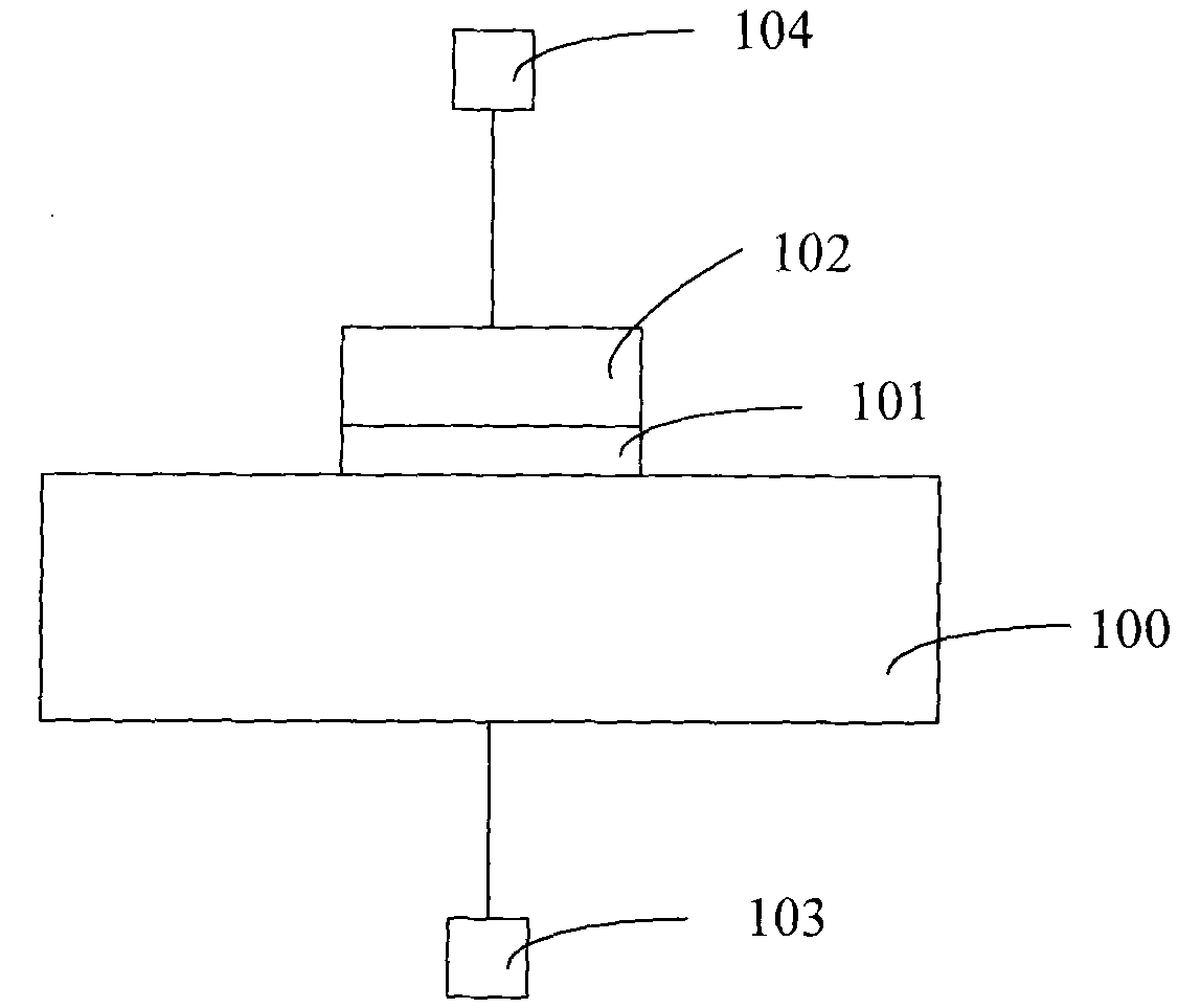
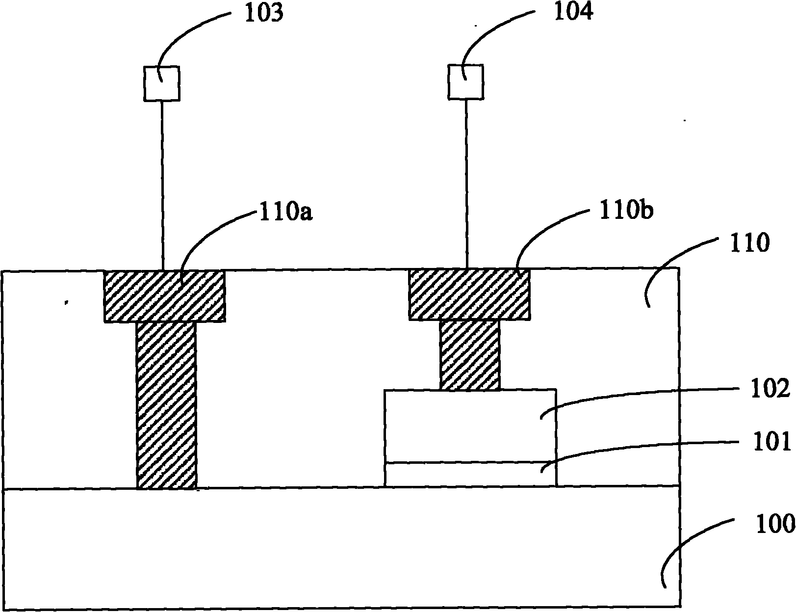
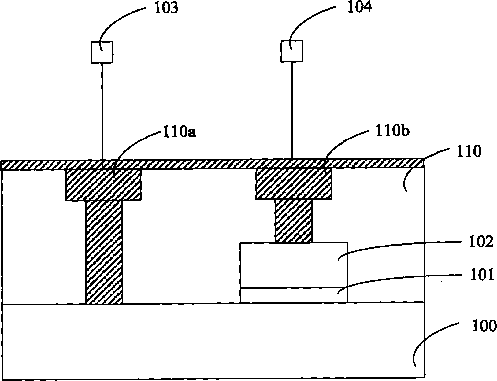
[0031] In actual production, such as image 3As shown, the pads 103 and 104 of the test structure are indirectly connected to the gate electrode 102 of the MOS transistor and the substrate 100 through the connection pads 110a and 110b in the metal interconnection layer. The forming process of the connection pads 110a and 110b mainly includes: forming an opening in the dielectric layer; filling the opening with metal to form a plug and a connection pad on the plug; during the filling process, part of the metal overflows the opening Covering the surface of the dielectric layer; grinding and removing the metal covering the surface of the dielectric layer by chemical mechanical polishing (CMP) to complete the formation process of the metal interconnection layer. During chemical mechanical polishing, if there is residual metal covering the surface of the dielectric layer after polishing, such as image 3 As shown, bridging defects between the connection pads in the metal interconn...


PUM


Abstract

The invention relates to a structure and method for testing the integrity of a grid oxide layer and a dielectric layer. The method for testing the integrity of the grid oxide layer comprises the following steps of: testing the integrity of the grid oxide layer through a first welding pad and a second welding pad, calibrating that a test result is in a passed state and finishing the test if the test is passed; or else, testing whether a short-circuited problem exists between the first welding pad and a third welding pad or between the second welding pad and the third welding pad; calibrating that the test result is in a passed state and finishing the test if the short-circuited problem exists; and calibrating that the test result is in a failed state and finishing the test if the short-circuited problem does not exist. The invention eliminates the interference of a short-circuited problem in a metal interaction layer on the test result and improves the test accuracy in testing the integrity of the grid oxide layer and the dielectric layer.

Description

technical field [0001] The invention relates to the field of semiconductor testing, in particular to a testing structure and testing method for the integrity of a gate oxide layer and a testing structure and testing method for the integrity of a dielectric layer. Background technique [0002] In the manufacturing process of a semiconductor device, in order to monitor the manufacturing process and ensure the reliability of the semiconductor device, it is common practice to form a test structure (testkey) in the device for testing some key parameters. In the CMOS process, the gate oxide layer (gate oxide) is an important structure in the device structure. The gate oxide layer should be an ideal dielectric layer without defects affecting its insulating properties. However, in the manufacturing process such as ion diffusion intrusion , Trapped charge and other factors will affect the quality of the gate oxide layer. [0003] The gate oxide integrity (GOI for short) test is a te...

Claims


Application Information

Patent Timeline
IPC IPC(8): H01L23/544H01L21/66
Inventor 周清华杨莉娟何莲群
Owner SEMICON MFG INT (SHANGHAI) CORP
Why Eureka
Try Eureka